Since starting work on the iPad 3 LCD, I have become fascinated with Retina displays. It’s crazy that you can pick up a panel that would until recently have cost hundreds or thousands for 60 bucks. Mass production is a beautiful thing sometimes. I may not be a Mac, but Apple gets my thanks for dragging the market out of the 1080p rut.
The only major issue with the iPad display is it’s less than ten inches diagonal. That’s very small for everyday use. They’re a nice portable size, but they’d look silly sitting on your desk as your primary monitor. Of course Apple makes a couple more Retina products which are better suited to everyday use. The largest of these is the display from the 15″ Macbook Pro Retina.
I believe my panel is from a Late 2012 Macbook Pro Retina 15″ unit. It is the LG version, model number LP154WT1(SJ)(A1). I bought two of them on eBay for pretty cheap as semi-damaged top assembly pulls from complete laptops. I ordered them about a week apart so only the first one has yet arrived. The unit arrived with a screwdriver crunch in the controller PCB and the internal copper planes are visible, so hopefully it works without shorting. Also the righthand cables were cut and there are two 3/8″ long quite deep scratches in one area. Well, I guess you get what you pay for.
First looks
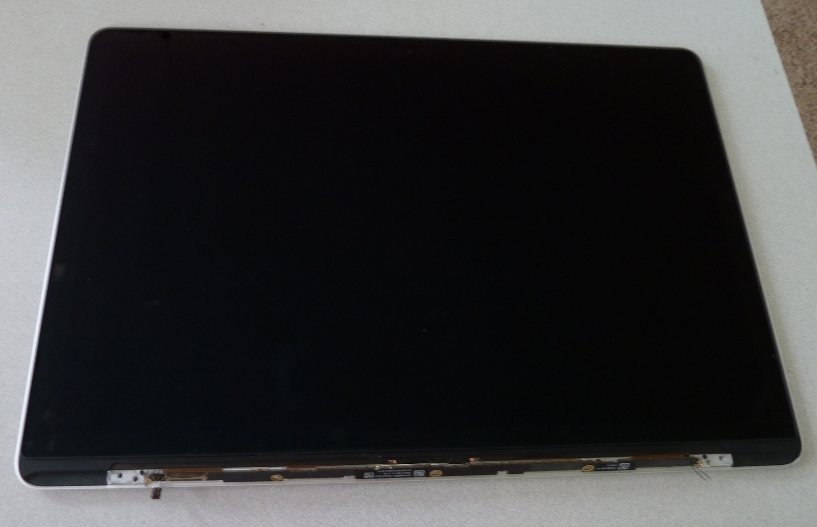
Macbook Pro 15″ Retina LCD assembly.
This really is a neat looking display. The glass spans practically edge to edge (although the active area is around a half inch inset inside that, more on top to accomodate the camera). According to the iFixit teardown, this assembly is only 7mm thick in the center with a panel glass thickness of 1.5mm. That’s mighty tiny, but also not as impressive as it at first sounds as the bare glass doesn’t include the backlight and diffuser that a normal LCD has – that’s part of the full display assembly. This is very important to note if you take up this project by purchasing one of the myriad bare-panel units on eBay – you’ll need to supply your own backlight, polarizer films and diffusers. This can get quite pricey and/or labor intensive.
The bottom of the LCD houses a black PCB which most people identify as an inverter, but this is in actuality the LCD control electronics and has no control over the backlight (more on this later). Inverter, in this case, is a misnomer anyway since the backlight is LED, and inverter topology backlight drivers are only applicable to CCFLs. But I digress.
The top of the LCD controller board is very sparse. Normally the WiFi/Bluetooth antenna array would be screwed to the top of this, so its lack of components was likely planned in order to prevent mechanical interference. What are present are two connectors, labeled CNT1 and CNT2.
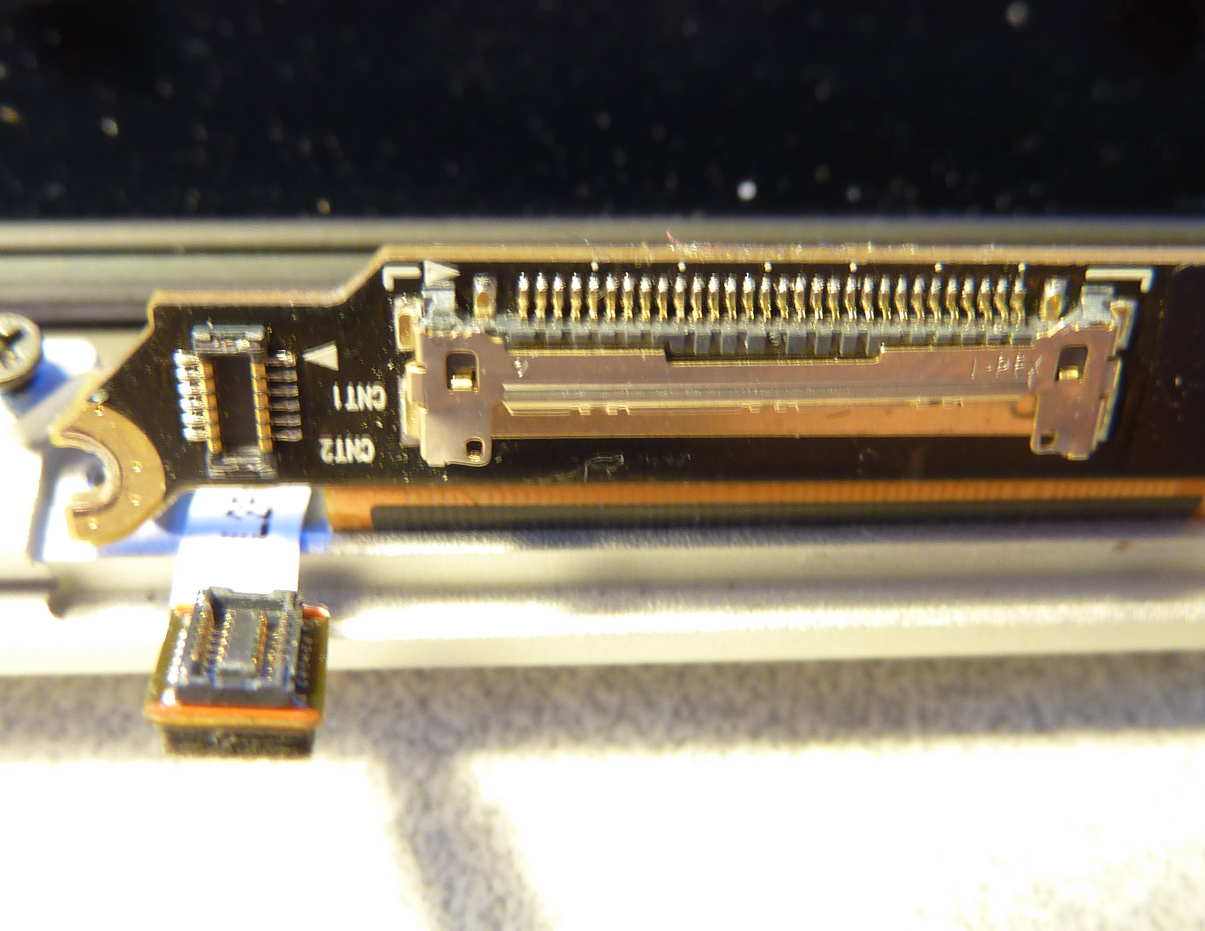
Connectors on the Macbook LCD assembly.
CNT2 is a 12-position dual row 0.4mm pitch board-to-board mezzanine connector with approximately 0.8mm stack height. I can’t seem to find the exact connector, but they are similar to Molex SlimStack connectors. CNT1 is the main LCD power and data connector, and is a 30-pin I-PEX Cabline connector.
The LCD controller is held in place by a screw at either end and two adhesive pads in the middle. In a complete assembly it would also be held in place by several additional screws which also affix the antenna array and the hinge cover, but these components were not present in the unit I purchased. Removing the screws and unsticking the adhesive pads, the guts of the controller are revealed. There are two metal shields covering the majority of the circuitry.

Detail of the backside of the Macbook LCD PCB. The metal shield covers have been removed.
Some of the ICs that are found:
- Parade Technologies DP635 LCD Timing Controller
- Integrated Memory Logic IML9660 Programmable LCD Calibrator
- Silicon Mitus SM4031 Display Power Management IC
- GD=EC 71L, 10-lead 3x3mm DFN (I believe this to be a Richtek DC-DC converter
though I can’t yet prove itProved it, it’s a Richtek RT8035) - 416R 8215, 8-lead 2x3mm DFN (I currently believe this to be an i2c EEPROM; there are SCL/SDA and WP testpoints nearby)
Naturally none of these things have datasheets available (EDIT: except for the RT8035!), but that’s okay, we really shouldn’t need them. This should be a self-sufficient display unit, which we should be able to feed power and DisplayPort to and it should just work with no further investigation. Hopefully.
Reverse-engineering the connectors
Unlike the iPad, I have been unable to locate a schematic for the Macbook Pro that explains the pinout of the connector. But from looking at how the iPad connector is built, and from investigating some more prominent features of the panel with a multimeter and a keen eye, it is possible to get quite far in the determination of the pinout.
Let’s begin with connector CNT2. We know that CNT2 goes to the display’s single backlight LED array from the iFixit teardown. This also tells us that there are 48 white LEDs in the array. This will become relevant in a moment.
On the main PCB, suspiciously nearby behind CNT2, is a 1206 ceramic capacitor, C103 (around 1.8-2.2uF, measured at 1.9uF). A bit of probing tells us that one end of the capacitor is tied to the gold-plated mounting pads for the screws, which is bound to be GND. The other end is tied to pins 5 and 6 (assuming pin 1 in upper right and pins numbered 1-6 top to bottom on right, 7-12 on left). Thus we can assume that pins 5 and 6 are the anode(s) of the LED array. More probing reveals that the two pins are also tied together in the mate connector, so we will assume that it is a single anode design.
Remember there are 48 LEDs in the array. The vast majority of LED drivers can only drive arrays that have equal numbers of LEDs in them. There are 10 remaining unknown pins on the backlight connector, but this is not an even divisor of 48. It is therefore quite likely for some of the pins to be no-connects, and for the LEDs to be split into series strings of 48, 24, 16, 12, 8, or 6 LEDs depending on the number of cathode connections present. It is difficult to determine the cathode connections at this point, so we change focus.
Let’s take a look at CNT1. We can assume that if this display is in fact eDP as everyone says, this connector is required to have the following:
- 4 lanes / 8 pins DisplayPort data (high resolution displays such as this will use all 4 lanes)
- 2 pins Aux channel
- 1 pin Hot Plug Detect
- At least one +V pin (probably several)
- At least one ground (probably several)
- Backlight control – either:
- anode and cathode connections from an off-board LED driver, or
- PWM, power and enable signals for an on-board LED driver
As a shot in the dark, I probed the connector to determine whether it happened to contain connections to the LED anodes as previously discovered, and sure enough, pin 1 was connected. Followup probing revealed that pins 3-8 were connected to pins 12-7 of CNT2. So it is apparent that the backlight driver for this panel is housed off-board, and that there are six driven strings that make up the backlight. This means there are 8 white LEDs per string, and if they consume around 3.2-3.4V apiece (common for white LEDs), the strings need to be driven with 25.6-27.2V each. We’ll file this knowledge away for a while.
We know that the mount/screw pads should always be GND, so this is where we turn next. Probing the connector for continuity to a mount pad, we find that pins 13, 16, 19, 22, 25, 26, and 27 are GND. This arrangement provides some further insight: There are three GND pads at the righthand side, which are likely the main power GND connections. Also every third pad is a GND for a long period. It is very common to separate high-speed signal lines with a GND connection, so we can guess that the four DisplayPort lanes can be found between the remaining GNDs. We’ll confirm that in a moment.
We now know where power GND is located, and there are three unknown pads adjacent which are very likely to be +V. This can be verified easily, as there is a 3A/32V fuse (F1) on the rear of the panel. As there are no other fuses present nearby, we can assume that this is the fuse for the power input, and measuring continuity between it and the connector yields that much as expected, the last three pins (28, 29, and 30) are +V. We don’t have a way of knowing yet how much +V is, but at least we know where it is.
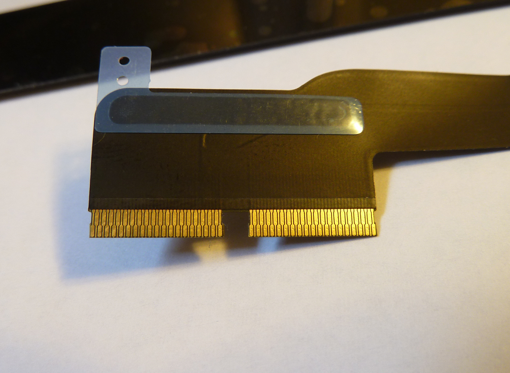
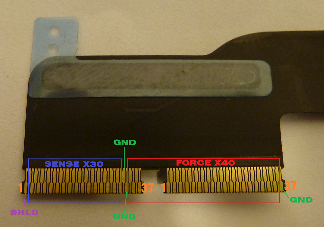
It is assumed that pins 14-15, 17-18, 20-21, and 23-24 are the DisplayPort lanes, but we don’t know for sure. For this, I unwrapped one end of the I-PEX cable that runs through the hinge to look at how the wires were arranged. A twisted pair or coaxial line would certainly mean high-speed data. As predicted, removing the (very well adhered) black adhesive cloth and desoldering some of the connector casing revealed four coaxial pairs on the pins in question. The connector also showed that the righthand pin of each pair has an insulated coating whereas the lefthand does not. I arbitrarily assume that the insulated wire is data+, and the uninsulated is data-, but verification of this is needed.
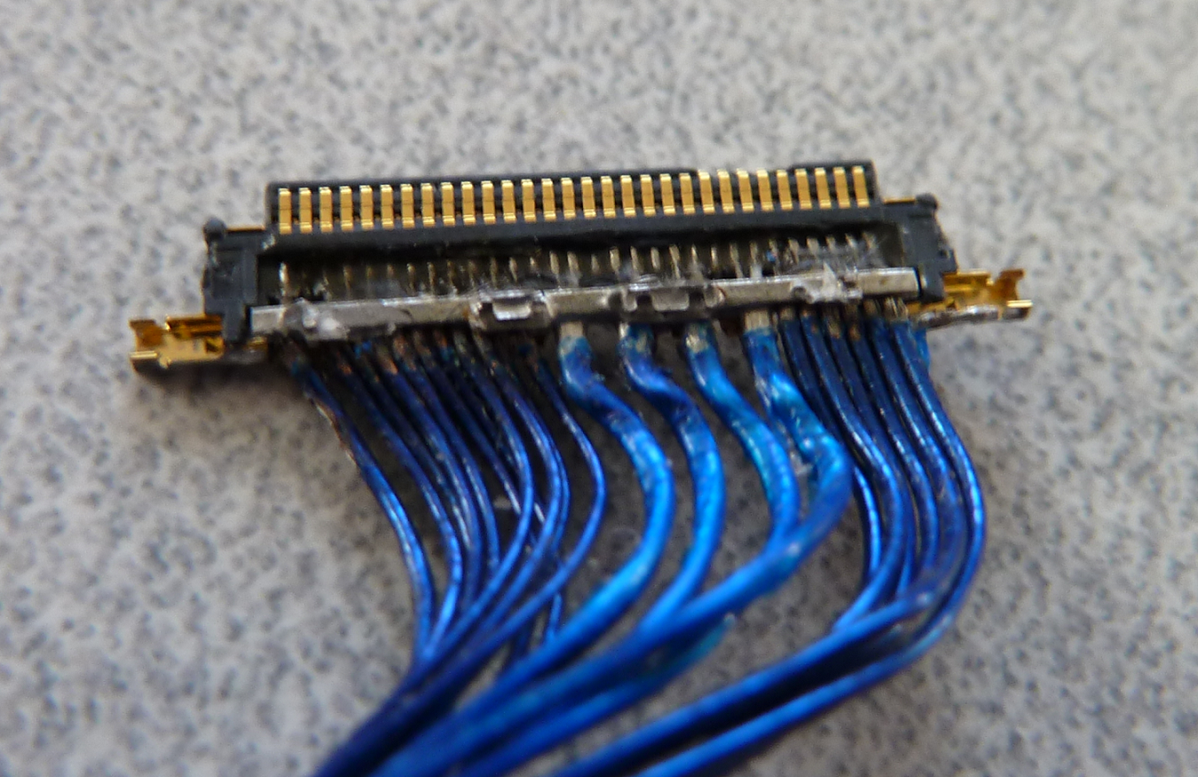
Macbook Pro 15″ Retina LCD cable, slightly disassembled.
There are now five unaccounted-for pins in the connector. One is pin 2, in the middle of the LED anodes and cathodes; we can assume that this pin is no-connect as no wire appears to be populated in the cable. The remaining four (pins 9, 10, 11, and 12) must map to three remaining required pins: AUX+, AUX-, and Hot Plug Detect. It is unknown what the fourth pin is for, but it is wired in the connector. It will be difficult or impossible to figure out which is which with simple probing. It will similarly be difficult or impossible to determine the order of the DisplayPort lanes. At this point there is no additional investigation that can be done prior to applying power to the panel.
Next steps
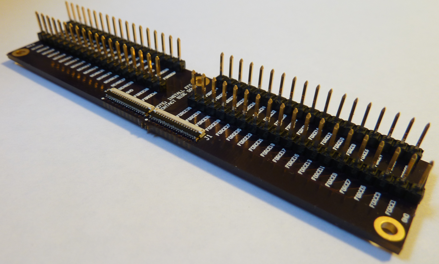
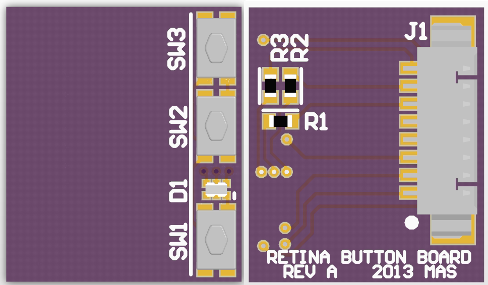
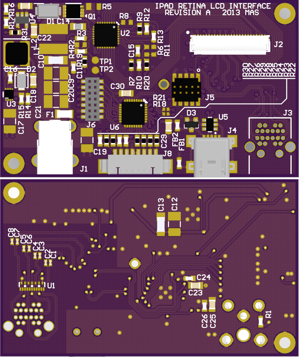
The I-PEX cable assembly is built through the hinge of the MacBook. As such they are very expensive to buy individually, so I don’t want to damage or cut the cable, and even if I did, soldering the very, very small 40AWG wires would be a nightmare. I am therefore designing a very simple board that breaks out the connector to pin headers. On the same board I will also place a mini DisplayPort connector connected to pin headers, so I can use jumper wires to test different pin configurations very quickly and easily to determine the complete and correct pinout. I do not plan to offer the documents for this PCB because it will only be useful for one test, and after I figure out the pinout I will be spinning a proper board with properly-routed matched-impedance connections. So stay tuned for that.
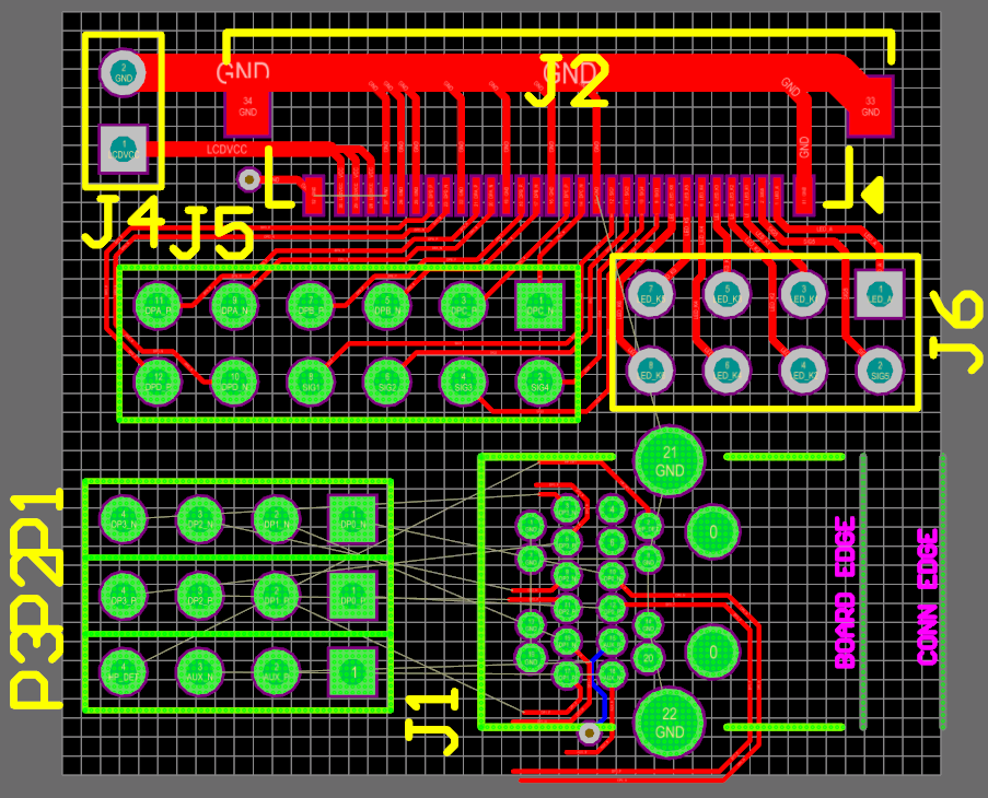
Macbook LCD test board, design in progress.
More on this when more is discovered.