Monthly Archives: April 2013

Investigating the iPad 3 Touch Panel, Part 1: First Looks

I mentioned in the initial post of the iPad 3 LCD project log that I purchased an iPad 3 digitizer in addition to the LCD.  I don’t want to call this article “Hacking” the iPad 3 Touch Panel, because I’m not sure how far I’ll get with it.  But I want to at least make a page for this in case my findings may be useful for anyone attempting a similar project.

The full digitizer, as seen from the back.

The full digitizer, as seen from the back.

This is a digitizer for the 9.7″ iPad 3 display panel.  It is, per Apple’s website, “capacitive multitouch”, although the particular type of capacitive is undocumented.  It is likely to be projected capacitive or some derivative thereof.  The connector at the center is a 2×37 pin, 0.3mm pitch FFC.  The contacts are on only one side of the flex cable, so a connector such as Molex 503566-3700 should be compatible.

2x37 pin, 0.3mm FFC.  Quite small.

2×37 pin, 0.3mm FFC. Quite small.

The cable does not appear to have any embedded electronics.  It is connected to the digitizer for about three tenths of an inch at bottom left and right in the above photo (top left and bottom left in the assembled iPad), and is glued down and appears to be occasionally connected along the remainder of the length.  Looking closely at the connection points, we can see how the contacts are structured:

Righthand contact interface.  This would be at the upper left corner of the assembled iPad.

One contact interface. This would be at the upper left corner of the assembled iPad.  Comes complete with dust under protective plastic film, and has been customized with black fibers.

The contact structure of the transparent section of the panel is typical of a mutual type projected capacitance design.  Forty-one very fine wiggly lines travel unbroken from left to right across the iPad display, while thirty rectangular contacts along top and bottom (as seen above) frame four short wiggly horizontal line segments between each unbroken horizontal line.  All horizontal lines terminate at a single contact on the right side of the iPad display and are individually connected at the left; all columns of line segments are bounded at both top and bottom by rectangular contacts (but are not in physical contact with them).  I have tried to photograph the pattern with a microscope, but it is very difficult, so I have illustrated the basic idea below.

Pattern of sense lines on the iPad digitizer.  Note that the digitizer is shown here on its side.

Pattern of sense lines on the iPad digitizer. Note that the digitizer is shown here on its side.  Ignore the poor MSPaint rendering.

The effective resolution of this touch panel is then 41×30, but of course by interpolating between points a position can be calculated to much greater accuracy.  It also explains the number of pins on the connectors – with 74 available contacts and 41 row + 1 row common + 30 column, only 2 pins are yet to be identified – although much work remains to map the functions to the pins.

Things are already looking quite good for getting this panel to do something.  With a waveform generating MCU and a little math, this may well be workable.

That’s enough on that topic for today.  See you next time.

Next post in this series >>

Hacking the iPad 3 LCD, Part 2: eDP Routing

Wherein the trouble begins.

The mDP and FFC connectors arrived yesterday.  I have some mDP sources and peripherals so I’ve seen the connector plenty before, but when you look at it on its own in your palm, it just looks so small.  And then compared to that, the 0.3mm pitch FFC looks perfectly miniscule.

Teeny tiny.

Teeny tiny.

As I mentioned in a previous post, I plan to manufacture these boards through OSH Park.  They have somewhat stricter design rules than my usual board supplier, but they’re also less than 10% of the cost.  The rules at time of this writing stipulate 6 mil trace, 6 mil space, with 13-mil min drill and 7-mil annular ring, and no plated slots.

Here’s the problem.  The pins on a mDP connector are so tightly spaced that it’s hard to route with 6-mil traces, and because plated slots aren’t allowed, an even more roundabout path must be taken for Link 3 to avoid the now necessarily round shielding pads.  I then spent a couple hours figuring out the optimal way to route the signals through the transient suppression diode array, got everything lined up and happily routed on one layer, and went to verify the orientation of the connector to the FFC, and…

Damn.  The pin numbering of the FFC is opposite that of Molex’s numbering for the connector!  Ugh!  Now all of the signals are backward.  And to maintain the desired relative orientation of the board to the FFC to the mDP, I cannot route it on a single layer anymore.  I knew it was too good to be true.

So be it.  The board is still routeable.  Just now there are vias in the high-speed lines, which is generally a no-no.  Well, you do what you gotta do.  Here’s my plan of attack:

Veeery preliminary.

Veeery preliminary.

I always start a design this way, by planning out the routes with regular (non-diff-paired, non-length-matched) traces and rough part placement.  Then I start a brand-new PCB and add in the parts and traces for real.  That way I don’t waste so much time with tiny tweaks and shifts, which is easily the most time-consuming and least satisfying part of a design for me.  So nobody write angry comments about mismatched trace lengths or pair separation, okay?

Every step of this process makes me more and more nervous about this design.  The capacitors in the above layout are 0402 size.  The occupied space is about one square inch.  The board will of course be much larger than this once I add the backlight driver, but still… I always have a hard time visualizing just how small a design is until it’s actually in my hand.  And this is easily the most intricate design I’ve yet done (most of what I do is big power stuff), so it should be even more surprising.

The work continues.  Hopefully I will receive the panel within the next couple days and I can get some proper measurements.

<< Previous post in this seriesNext post in this series >>

Hacking the iPad 3 LCD, Part 1: Component Choices

In the previous post I laid out some of my plans for implementing the interface board for the iPad 3 LCD.  In the meantime, I have done some (or rather, quite a lot of) research on the subject, and have gained some additional insight into what may be involved.  I have also begun to choose components based on what I know about the (still en route) panel.

Basic physical attributes

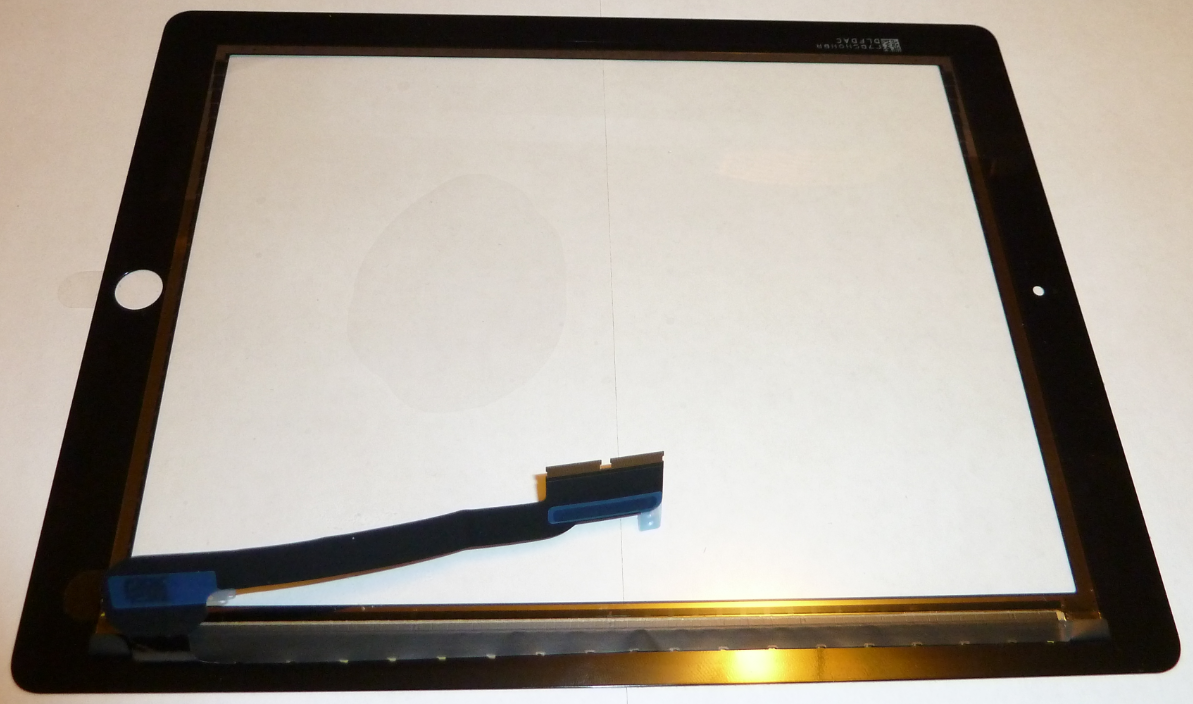
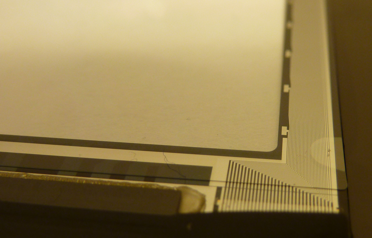
As a panel designed for assembly in a greater structure rather than being self-supporting, there appears to be little in the way of mounting provisions.  I vastly prefer screw-based mounting to any other method for ease of manufacture and the ability to remove pieces to work on them without damage, but in this case the only way that would be feasible would be if the board were some seven or eight inches wide (enough to span one entire edge of the display), and I don’t plan to build enough into the board to need that much space.  Furthermore, this would still only be two mount points, leaving the board unsupported toward the center of the panel.

For now, the ideal mounting method appears to be double-sided foam tape.  It’s cheap, it holds reasonably well but not TOO well, and it’s thick enough to hold through-hole component leads just a little bit off of the rear metal surface of the display panel.  The board will be affixed to the upper left corner of the rear, such that the eDP tail mates up with the connector without too much fuss.  I know this kind of clashes with my “must be elegant” mantra, but it will have to do until I have the opportunity to do up a “proper” back casing (which will have to wait until my budget allows me to buy a mini-mill).

At the moment, I am envisioning a board of dimensions no larger than 2×3.5 inches.  That should be plenty of space to work with without being too cramped.  Using OSH Park, that’s $70 for three boards.  Not exactly free, but not terrible for four-layer one-off prototypes.  Two-layer is more reasonable yet, but the boards will need the extra layers as it’s near impossible to produce a board with decent signal integrity in the 2GHz range in two layers.

Electromechanicals

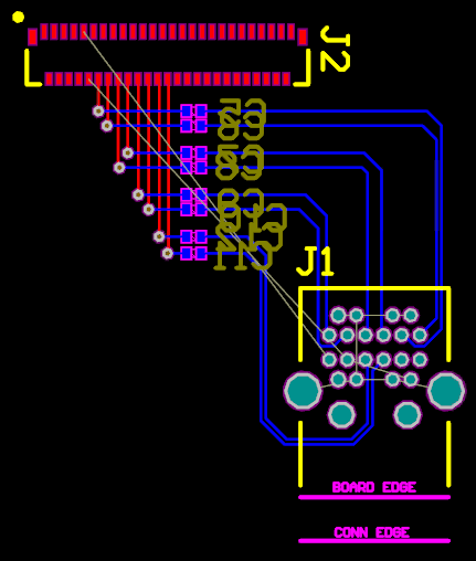
As I noted in the previous post on this topic, I would prefer not to solder a hacked-off wire to the board.  To that end, I will be connectorizing everything possible.  My choices in connectors are largely driven by what is available in onesies from the normal distributors – I don’t want to rely on samples of obscure parts, and I don’t have the buying power to request anything extravagant.

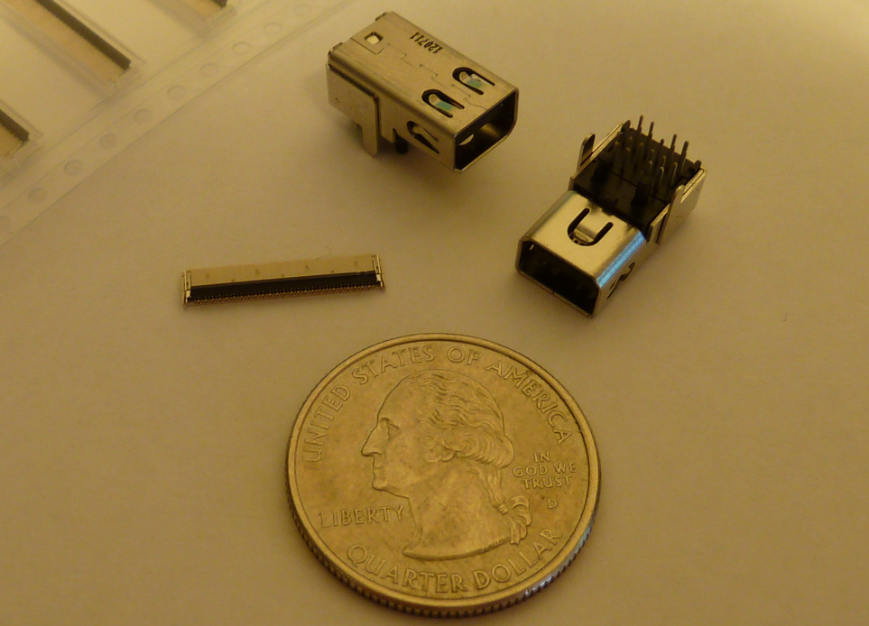
To bring signals into the control board, I will be using a miniDisplayPort connector.  They’re compact and electrically correct for this application.  They are also surprisingly hard to find, but Mouser currently has a healthy stock of Molex 105081-0001 so that seems like the winner.  It’s a through-hole part with fairly tight spacing so fanout might be interesting, but I’ll deal with that when I get there – there really aren’t many other options.

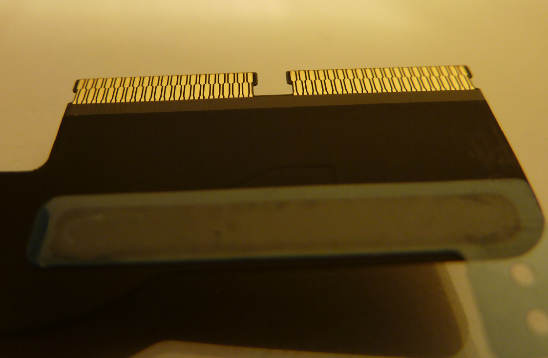
To get from the board to the panel, I have opted to forgo additional research and use the already-identified Molex 502250-5191 as documented on [Andrzej]’s original writeup.  I suspect there are plenty of other options out there, but I’ve always found Molex to be more readily available in the United States than any of the Japanese vendors’ parts (e.g. JAE) and I don’t think it’s worth bothering to find compatible connectors which I can’t buy.  These are also in stock at Mouser at time of writing.

I will be feeding my board with a 12V 1A adapter, similar to http://www.ebay.com/itm/360545176232.  These are provided with every small networking appliance and external hard drive, and I’ve got a billion of them.  I brought in some CUI PJ-047BH 2.5mmx6mm barrel jacks for a related project at work, and plan to use one of these to accept the 2.5×5.5mm barrel plug on the adapter.  (In-stock at Digikey)

Backlight driver

You’ve waded through the boring stuff, now on to the fun bits.  The panel has two banks of six common-anode LED strings for its backlight.  Per the panel datasheet, the strings are rated at 18.5mA, 4.4W.  This works out to a string voltage of 19.8V, higher than the voltage I am providing to the board.  I could have used a higher-voltage adapter, but I have plenty of 12V ones already.  So my requirements for the backlight driver are 12V in, 12 channels out at >= 18.5mA, max output voltage >=19.8V.

Many solutions call for a two-chip set – a boost switchmode supply to produce V+ for the LEDs, followed by a low-side-switch array to handle the PWM dimming.  I have instead opted to use a combined boost regulator and PWM controller, to save board real estate and complexity.

There are several options available in this arena – Atmel has a couple, Maxim has at least one – but I ultimately chose the Linear Technology LT3754.  I have used a lot of Linear parts over the years, and I think they have some of the best datasheets and application notes of any manufacturers.  Plus they have good field reps (Hi Bryan and Rynk!).

The LT3754 is a 16-channel boost-mode driver with 50mA string drive current and up to 45V string drive voltage from 4.5V input.  It can take a PWM dimming signal, or an analog voltage if you’re crafty.  Additionally, it’s not too expensive, there are less than 20 external components, and it comes in a compact 32-QFN package  All in all, a really neat device.  I made up a spreadsheet to calculate the parameters for the driver.  I may post it later once I clean it up a bit.

Backlight considerations

The identification of a feasible backlight driver brings up some thoughts from the previous post.  I now have a DisplayPort input and a PWM-controllable backlight driver, but nothing in the middle.  Where can we get backlight control information from?

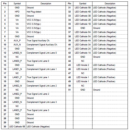
DisplayPort consists of four high speed data links and a low-speed control channel (“AUX”).  This AUX port has a number of interesting features.  In its simplest form, the AUX channel acts like the Display Data Channel of competing technologies (e.g. DVI, HDMI), informing the host of the resolutions and refresh rates and other key capabilities of attached devices (EDID).  However, it may also perform additional tasks – providing, for example, a channel for host-to-device control and configuration.  It is this function which is most interesting for this application.

DisplayPort supports the VESA Monitor Control Command Set over the AUX channel.  According to Wikipedia, a subpart of this standard supports backlight control.  If the data is sent to the panel, and we can decrypt and act upon that data, the operation of the monitor will be greatly improved beyond the otherwise sole option of manual backlight control.

But how do we get at the data, if it even exists?  There exist DisplayPort to LVDS receivers which break out this data (for instance, NXP’s PTN3460), but then we’re left with LVDS for a eDP panel.  Maybe we could buffer and split the DP signal to both our panel and the receiver IC, or convert from DP to LVDS and back to DP, but this starts to become expensive and space-consumptive and complicated.

Ideally we’d want to get at the backlight control data without bothering to retransmit the DP links.  In its basic form the AUX channel is a bidirectional half-duplex 1Mbps I2C-esque bus, which we can potentially read with a microcontroller.  The data is Manchester-encoded to be transmitted over twisted pair cabling though, so we need to decode the data, then interpret it.  It will be difficult to find a device that can do the interpretation in hardware as it has a nonstandard packet structure, which means we’d need either a decently-fast processor (to bit-bang it) or some sort of programmable logic.  So we’re in it for some semi-serious hardware and/or software to solve a simple problem.  Not exactly elegant, as per my design guidelines.

It is desirable to find an alternative source of this data, but so far other options have eluded me.  The search continues, but that’s enough for one day.

<< Previous post in this seriesNext post in this series >>

Hacking the iPad 3 LCD, Part 0: Planning

Today, a post on one of my favoritest sites (Hackaday) piqued my interest.  The post was titled Connect a Retina display to a regular computer.  I have always been a huge fan of high-resolution displays, but they have traditionally been far outside my price range.  But here, says the article, is a massively high resolution display, with simple drive characteristics, that can be had for only $55.

I bought some immediately.

The post links to the efforts of [Andrzej] and his post on the subject, http://emerythacks.blogspot.com/2013/04/connecting-ipad-retina-lcd-to-pc.html, and if he should ever happen to run across this page I sincerely thank him for his work in this area. But I am nothing if not a perfectionist, and happen to be an electrical engineer by trade with some high speed design experience, and I have been working on some very similar things at work, so it seems an excellent opportunity to improve upon the original design and make something a little cleaner.

So here’s the plan of attack.  While the displays make their way to my house, I will begin the design.  The display is a LG LP097QX1-SPA1, for which I have a half-Korean datasheet posted here: LP097QX1-SPA1.  (Edit:  A somewhat less Korean datasheet for the similar -SPC1: LP097QX1-SPC1)  The datasheet outlines the pinout of the display, in the following manner:

LP097QX1-SPA1_Pinout

Neato!  It’s just DisplayPort and power and LED strings.  We can deal with this.  DisplayPort means no pesky EDID EEPROMS, and no finicky LVDS data format issues.  Should be a cakewalk.  However it is also worth mentioning that what you see is what you get.  There is no capacitive touch interface here.  That is all found on the transparent glass digitizer normally attached to the front of this LCD.  A lot of people in various forums seem confused on that topic.  I purchased a digitizer as well, but I give no guarantees on how far I’ll get on that.

Based on [Andrzej]’s original writeup, I will be emulating his work while adhering to the following additional guidelines:

  1. I hate splicing wires.  I have done plenty of Apple Display Connector to DVI conversions (hint: topic of a future post), and I really hate having to splice itty bitty wires.  It’s also a great testament to the hardiness of DVI that the display works with such a simple fix, as the resultant signal looks horrid.  I don’t have so much faith in the higher-frequency DisplayPort signals, so I will be designing the solution with a standard mDP connector onboard.
  2. Driving LCDs with a constant-voltage supply is not ideal.  I know it works, but LEDs are constant-current devices and are either hard to drive adequately or easy to overdrive with a constant-voltage supply.  I have designed a reference circuit for a six-channel LED driver for a project at work, and will attempt to adapt this to the 12 strings of this display.
  3. Everything worth doing is worth doing right.  If it’s not worth doing right, it’s not worth doing.  This is really the most important thing to remember about this and every project.  I really hate half-arsing projects, so much so that many of my projects have been put on semi-permanent hold if they fail to live up to the initial elegance expected of them.  This mod should provide an elegant, highly usable, production-quality end product, or I just won’t end up using it.

I believe my plans to be reasonably sound, but I do have a few nagging questions remaining, primarily concerning the backlight.  In a traditional embedded system, the display controller has control over the backlight state and brightness, and wiggles the controls of the backlight driver to its whims.  In a commercial DP monitor, the monitor’s display controller pulls this information from the DP data.  But in this application, the DP signal data is simply passed through from input connector to panel, no post-processing included, and no additional backlight controls are presented, so presumably the backlight will be on all the time (which is undesirable).  IPS displays are thankfully naturally black, but that’s no real consolation for a system being designed as elegantly as possible.  I will need to investigate this issue when the panels arrive.  I also need to think through backlight brightness adjustment, because again no backlight level control data is exposed.

Next step is to start blocking out the main components of the interface board.  As I have nothing yet to show, I’ll leave that for the next post, so that’s it for now.  Thanks for watching!

Next post in this series >>