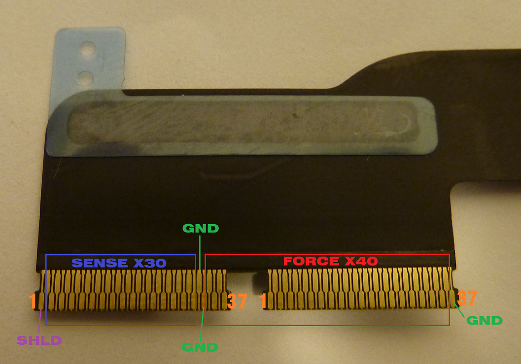
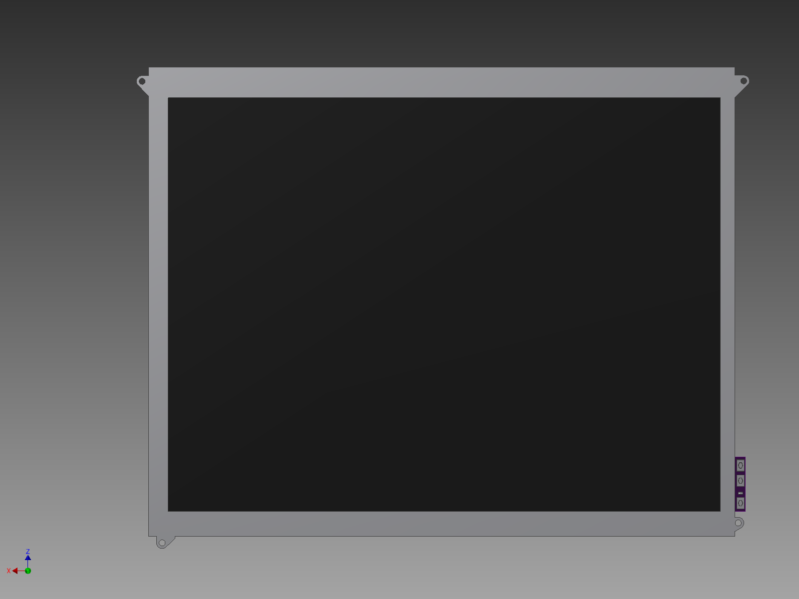
The digitizer breakout boards arrived, signalling a new round of experimentation with the iPad 3 touch panel. The design of the board seems mostly solid but for a couple of issues. First, as predicted, the edges of the digitizer FFCs need to be trimmed off for them to fit in the connector. This is easily done by pressing down on the FFC on a hard surface with a sturdy sharp knife; the semi-brittle stiffener separates cleanly and without bending the contact portion of the cable.
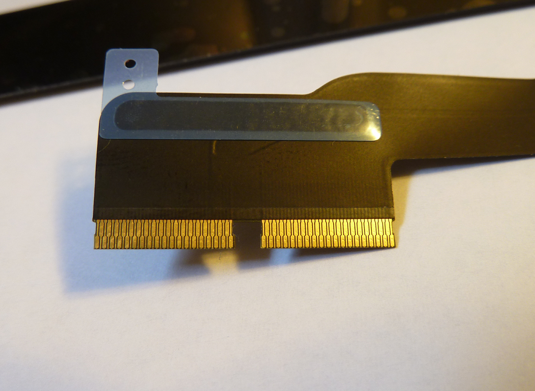
The connectors used on the breakout need the FFC trimmed just shy of the contacts, but this is easy to do.
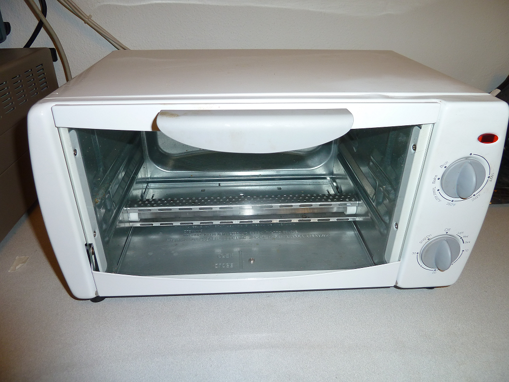
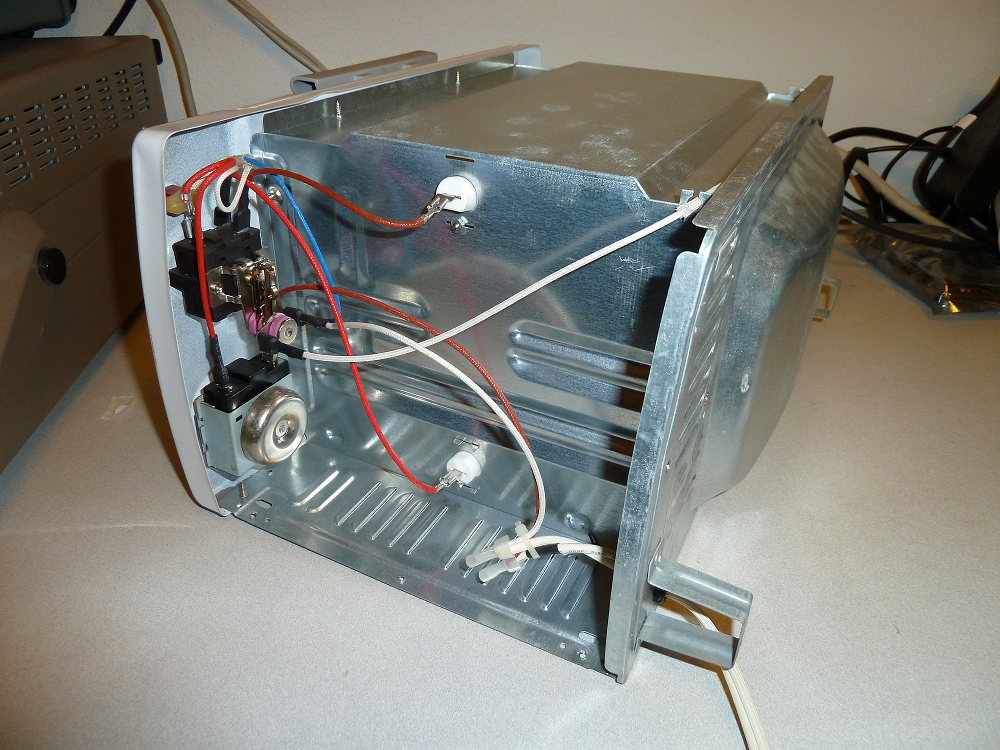
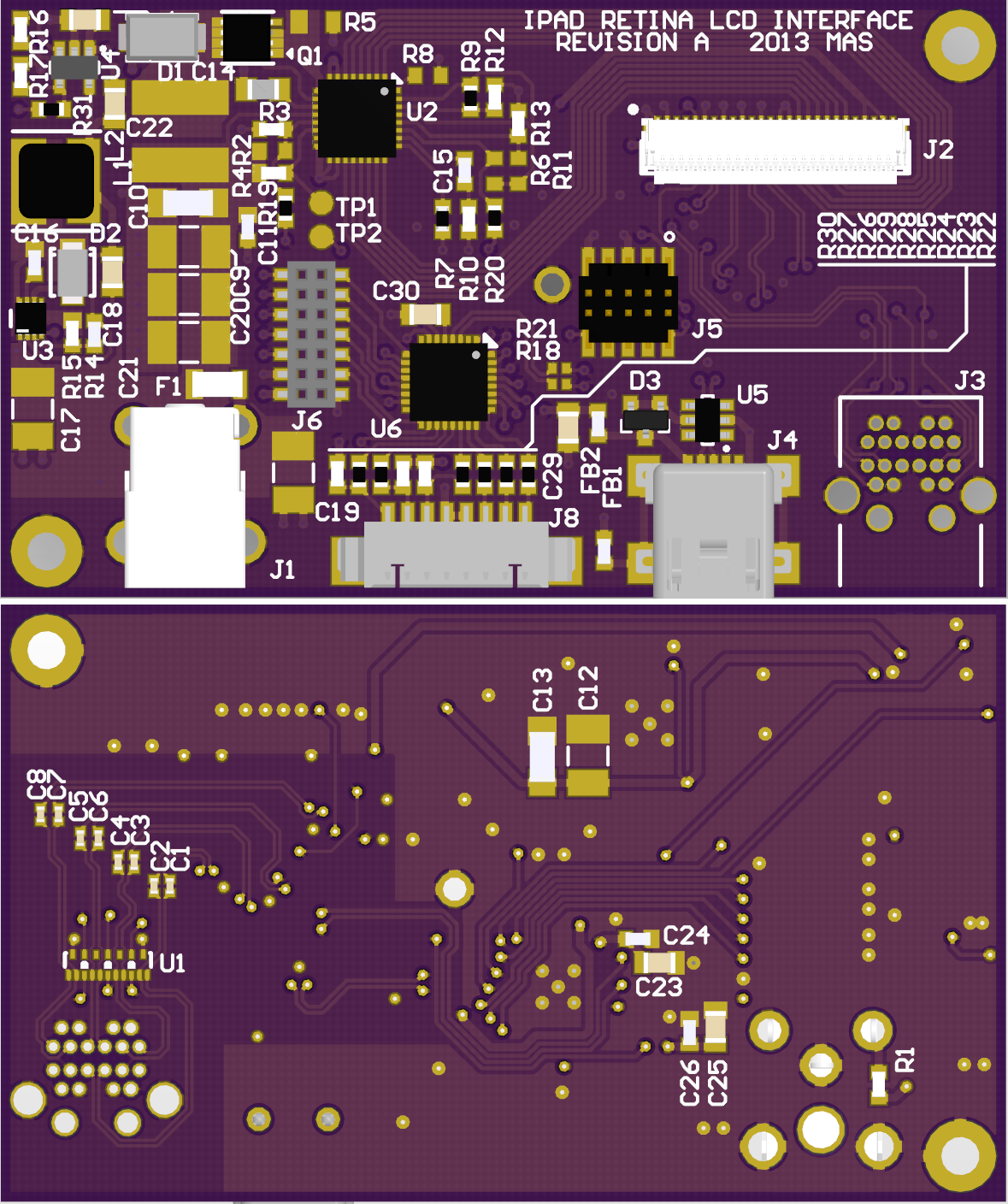
I reflow soldered the board by manually controlling the guts of my toaster-turned-reflow-oven, which worked quite well. I would be cautious to try hand-soldering the tiny connectors as alignment is extremely important, but it might not be a terrible idea, particularly if you don’t have infinite time and patience – I did not have a stencil and individually applying the proper amount of solder paste to each of the 78 miniscule pads took nearly two hours. But the result works beautifully, so I consider it worth the time – plus I got to experiment with a method I’ll need to use a lot when I start building the other boards. Tip: Sharpen a wooden toothpick to use as an applicator. I tried metal points and had a lot of trouble.
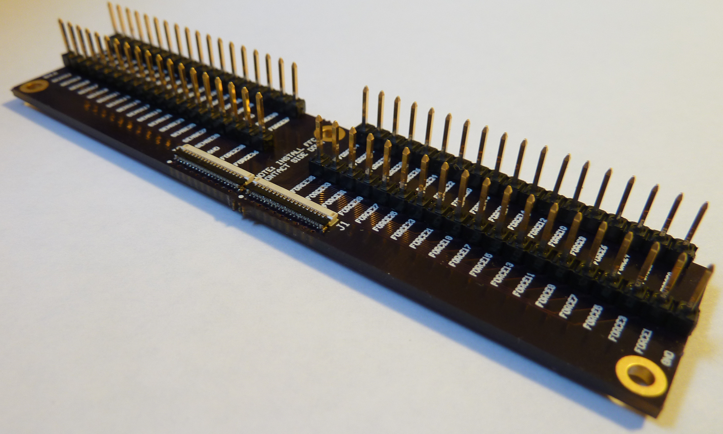
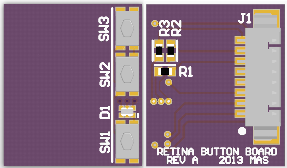
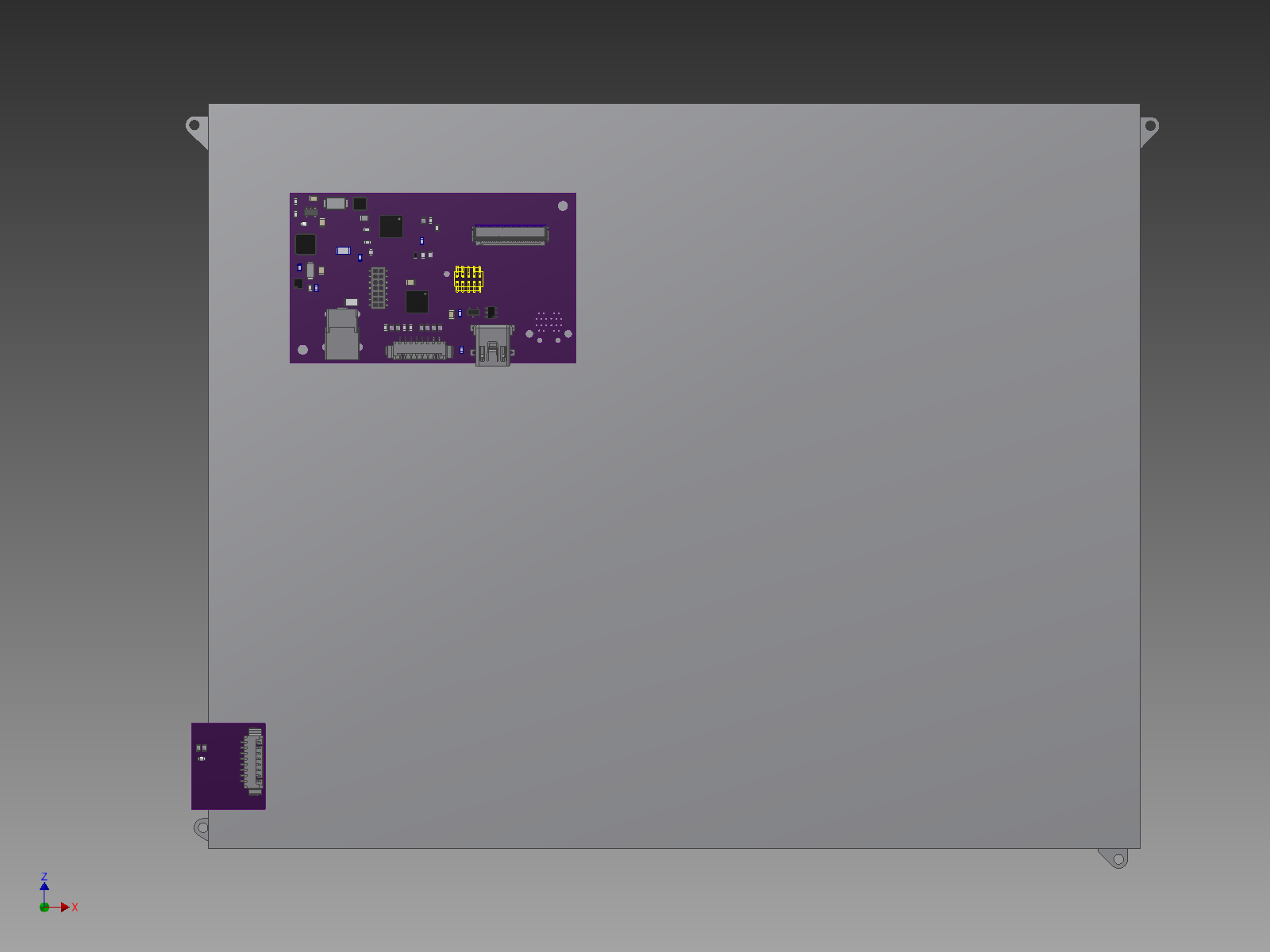
The completed breakout. This one has the pins set up for breadboard use.
The other issue with the board is that it overhangs four breadboard rows beyond the connection row, so it’s not impossible but certainly difficult to connect to the row of pins toward the FFC connectors. Again though, this is not meant to be an end-all solution, just something to facilitate probing the digitizer until a real board is built, so I’m not too upset about it. Plus the board could not be made much narrower without disrupting the currently-zenlike layout of traces.
As I now have a way to get into the connectors, I’ve done some more experimentation with the panel and have come to realize that much of what I thought I knew about the driving of this panel is wrong. I have stared at the pictorial diagram of the concept of mutual pcap for many tens of minutes, but it never clicked until I started playing with the digitizer. The key is this: the capacitance of the display isn’t directly sensed! No relaxation oscillators here, the pictorial says it all – mutual pcap uses your body capacitance to prevent some of the electric field from coupling from the driven lines to the sense lines!
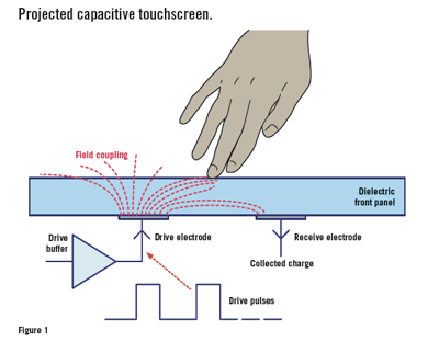
It took me an embarrassingly long time to register what is happening here.
Using the breakout, it is easy to see how this works. Using a function generator, I drove an 18V square wave into FORCE0 through a resistor (value dependent on frequency used) and connected generator common to the GND pins. Take note, Apple drives the digitizer with approximately 18V in the iPad also. I then connected an oscilloscope to SENSE28 referenced to GND, and grounded SHLD. The result was a mirror of the input signal at an amplitude of approximately 330mV coupled onto the sense line. Then, when the bottom right corner of the digitizer is touched (this is the cross point of FORCE0 and SENSE28), a visible 30mV drop in amplitude shows up on the sensed waveform.

Initial breadboard setup of the digitizer test board.
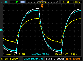
Waveform capture of a 72KHz signal driven through a 10K resistor into FORCE0, coupling into SENSE28. Yellow is source, white is sense without touch, cyan is sense with touch. A clear difference can be seen between touch and no touch.
Now, 30mV may not seem like a lot, but against 330mV that’s just over 9%, which should certainly be detectable. In fact, if we fed this signal directly to a 3.3V-referenced 12-bit ADC, this would be around 40 steps of difference, which may be detectable with ample averaging. But we can do better than that. By using op amps to amplify the signal to the 3.3V range (and to DC bias it up above ground for better compatibility with ADCs), we should have plenty of dynamic range to sense touches.
This is where I hit a snag. I figure that for 40 force lines and 30 sense lines, and desiring a refresh rate equal to the LCD itself (60Hz) to prevent sluggishness, a touch scan rate of 40*30*60=72KHz is the minimum necessary. If averaging is desired for better accuracy, then scan rate will need to be a multiple of this. However, I only had general purpose op amps on hand, with slew rates in the 0.5V/us range. In the 70+KHz range, square wave edges over a 0.5V/us slew rate device are just too slow compared to the small differences we are looking for. I will need to source some higher-speed op amps before I can really try this out.
But until that happens, here is my plan for interfacing the digitizer. I will use some programmable logic or a few 4:16 decoders to drive an array of transistors connected to the force lines, which will generate a pulse on each line in turn. An analog mux will pipe all 30 sense channels into a high-speed op amp and then into a megafast ADC which will continuously scan until a certain voltage level has been reached. If the pulse generation time and the minimum level received time are a known distance apart, it should be trivial to determine whether the screen is being touched in this area – the longer it takes to reach the desired voltage, the more charge is being diverted into the attached capacitive body (e.g. finger). An array of op amps and a couple of multichannel ADCs could be used in place of the multiplexer as well if that ends up being less expensive or more accurate.
Now awaits another trip to Digikey and some more research, but this is starting to look more and more feasible.