Monthly Archives: March 2015

Weekend Project: Macbook Pro Camera Investigation

A while back, I wrote an article on the camera in the Apple Macbook Pro A1398 lid assembly.  In that article, I published the pinout of the FaceTime camera in the lid, and demonstrated how it could be wired directly to USB and function as a generic USB webcam – but not a very cheap one, since the panel assemblies are still pretty expensive.

Well, it turns out that you can buy the bare camera module for a very reasonable $5 at everybody’s favorite auction site.  A visitor to this site wanted to use these cameras in a standalone application and offered to send me one to play with, in return for a little bit of investigative work.  Sounds like fun, let’s take a look.

Macbook A1398 camera module, first front...

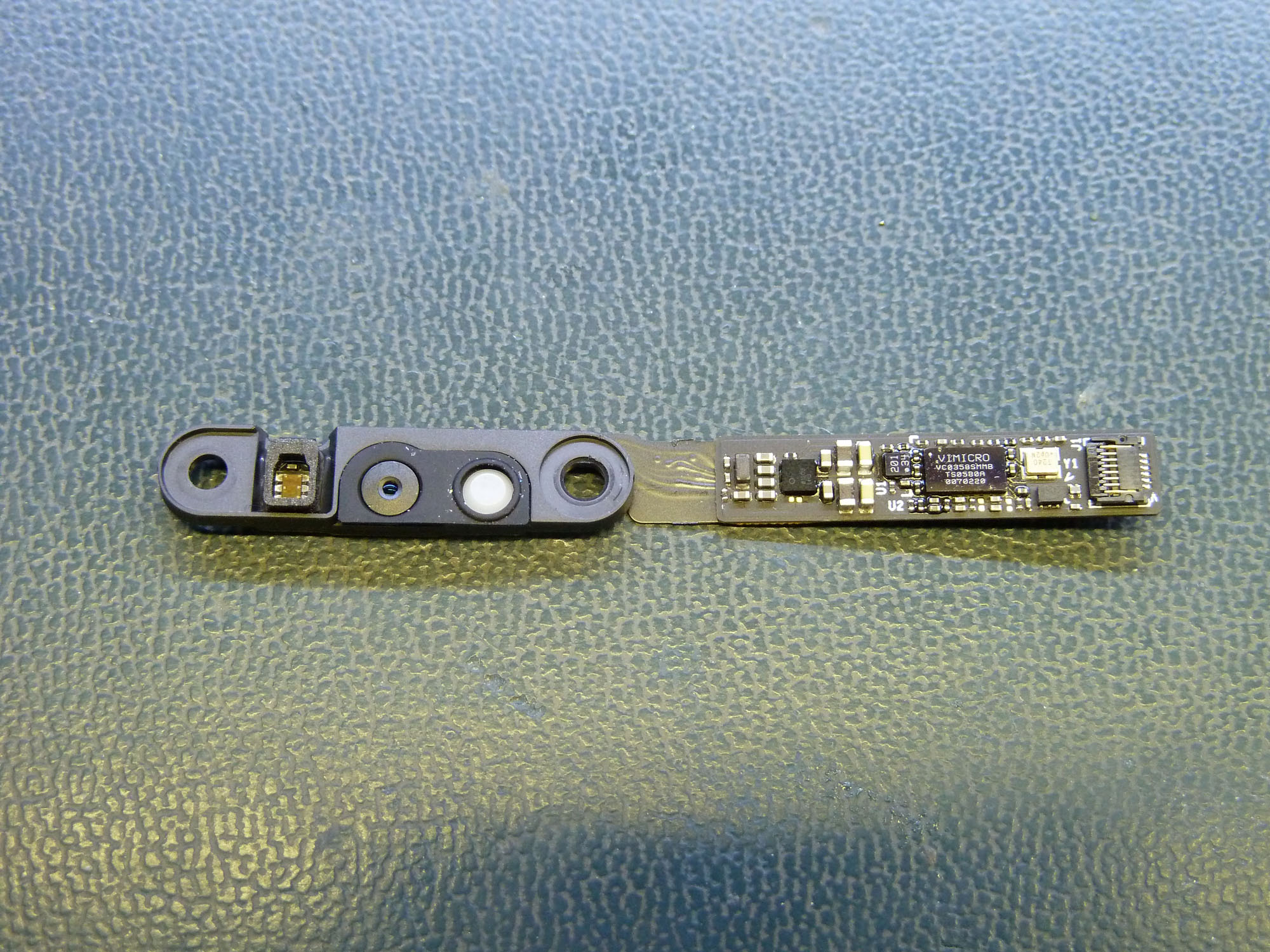
Macbook A1398 camera module, first front…
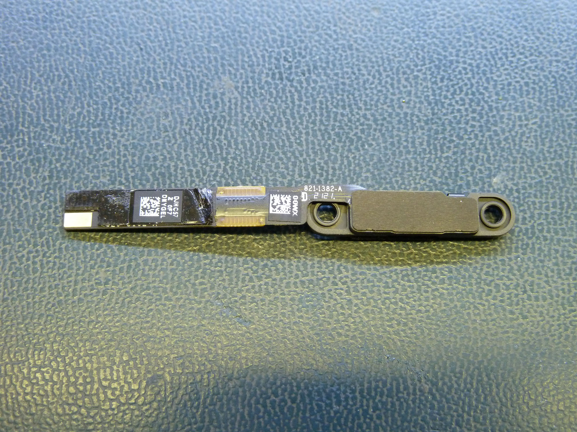
...then back.

…then back.

As a recap from last time, note that this module contains not only the camera but also the laptop’s ambient light sensor (seen at left on the front view).  There is a little foam ring around the ALS to prevent errant readings caused by the LCD backlight or the camera activity light.  Next to the right is the camera lens, and the white circle is the activity light.  The camera sensor and the ALS are on a little flex PCB which is soldered to the rigid board containing the rest of the circuitry.  Many of Apple’s other assemblies are made as a single rigid-flex assembly, but the two cameras I’ve investigated have both had separate control and sensor sub-boards.  I wonder if the camera assemblies would otherwise be damaged in reflow.

The top of the control board houses a VIMICRO VC0358SMMB.  We can assume that this is similar to the VIMICRO VC0358PQNB, for which there is a public data brief (PDF), but this part is in a wafer-level BGA package instead of LQFP.  The suggested SPI memory is probably present as the 6-pin device to the lower right, and presumably contains the USB descriptors identifying this part as a FaceTime camera.  The other WLCSP to the left looks suspiciously like some sort of voltage regulator, though I didn’t bother to measure the nearby capacitor voltages to verify that.  Note that although the VC0358 has microphone input capability, this board does not appear to contain a microphone.

The input connector is on the righthand side of the board as seen in the front view.  The connector is a 6-pin, 0.4mm-pitch FFC receiver.  I probed around the board and determined the pinout of the connector to be the same as it is on the motherboard side of the harness (pin 1 is marked with an arrow):

Pin Name Description
1 GND USB/ALS Ground
2 D+ USB Data Positive
3 D- USB Data Negative
4 +5V USB/ALS Voltage In (+5V)
5 ALS_SCL Ambient Light Sensor I2C Clock
6 ALS_SDA Ambient Light Sensor I2C Data

This is all well and good, but soldering to the 0.4mm connector is an absolute nightmare.  It’s not something the average person is going to want to attempt.  We could buy a little FFC jumper to plug in, but if we only paid $5 for the camera, having to buy more parts would negate that cheapness.  Thankfully, if we remove the sticker from the rear of the module, the manufacturer has left us plenty of testpoints.  I mapped the ones that connect to the connector pins, and came up with the following pinout:

Testpoints on the rear of the camera module

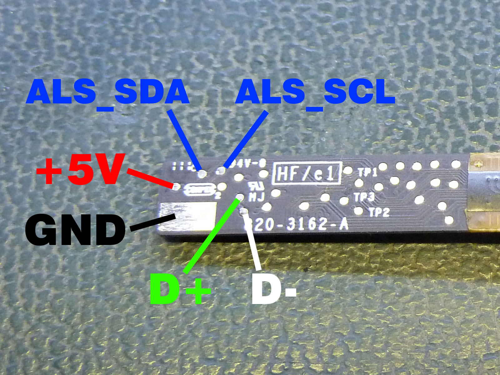
Testpoints on the rear of the camera module.

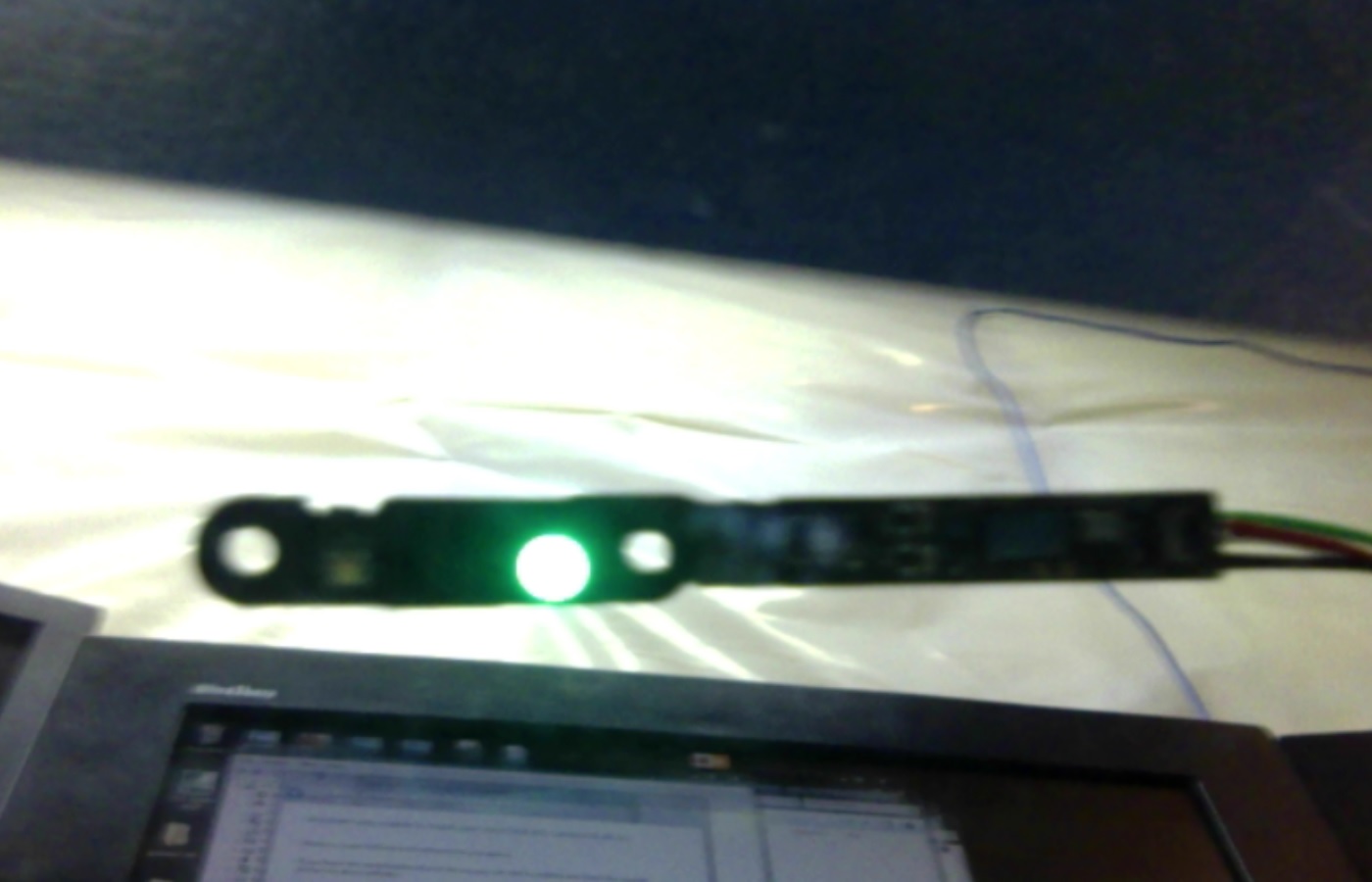
Using this scheme, I soldered on an old cut-off USB cable:

Camera wired as per the testpoint map above.

Camera wired as per the testpoint map above.  The ALS pins have not been connected.

And what do you know, as soon as it was plugged in the camera was recognized the same way it was in the previous post – as a USB Composite device containing two FaceTime HD Camera devices.  Again, as last time, one of the two devices has no available driver, but the camera works just fine with only one of its sub-devices installed:

The camera takes a selfie.  Note that it's blurry mostly because I had to hold it and take a screenshot at the same time.

The camera takes a selfie. It’s a bit blurry, possibly because it can’t properly focus at this range.  I didn’t notice that when I was taking the photo, oops.

So there you go.  If you need a cheap and small USB camera for something, these are pretty easy to hack onto.  Hopefully this is useful to somebody!

Weekend Project: A Tiny Core Memory Array

Remember magnetic core memory?  Maybe you don’t, if you weren’t around in the ’50s or ’60s (or aren’t a tech junkie like me).  But it was one of the key developments during the evolution of the modern computer.  At a time when large scale integration on silicon was just beginning and massive silicon memories were infeasible, core memory fulfilled a critical need for larger, faster memories for some of the early big-iron mainframes.

Core memory is interesting because it’s one of the simpler memory constructs to understand, even today.  The basis of the system is a humble ferrite ring (a “core”).  The core material is formulated to exhibit high magnetic remanence – that is, it retains a magnetic field very well.  By utilizing Ampère’s law and passing a pulse of current through a wire threaded through the center of the core, a persistent magnetic field can be induced.  Applying Faraday’s Law, it is then possible to “read out” the state of the core – if the core already has had a field induced within it, then passing another current pulse has no effect; otherwise, a slight voltage pulse is developed across any wires passing through it,, which can be measured.

Expanding the scope a bit, it is possible to write to and read from a large quantity of cores if they are arranged on a two-dimensional grid.  As a result of the particular magnetic properties of the cores, they only change state when a sufficiently large current is passed through them.  This current can be split to any arbitrary number of wires; as long as the sum of the currents is above the minimum for the material, the field is induced.  If we pass half the necessary current through one row of a two-dimensional array of cores, and half the necessary current through one column of the same array, we can affect only one chosen core in the array.  An additional wire passing through all cores is typically used to detect the state of the chosen core.

I have an ambitious design in mind which will get a more detailed post later, but suffice it to say for now that I’m planning a combination art and engineering project which needs a bank of memory.  I could go the simple route and put a simple DIP SRAM in, but that’s no fun to look at.  But I bought a little can of 50,000 memory cores a few years ago, and that seems like it might be a little more fun.  That’s enough for a 4KB array, which ought to be enough for what I’m planning.  But before I spend several weeks building a 32,000 core array, it’s important to understand how the assembly will work.  To that end, I’ve planned a few baby-steps to build up to the real deal.

I’ve designed a simple PCB with a large route-out in the center and an array of holes around the outside.  The board is designed as a carrier for a small 8×8 array of cores and their associated wiring.  Because my application calls for byte-addressable memory, the eventual plan is to stack eight such boards to support parallel access of an entire byte, but at this point testing will begin with a single 64-bit array.

There's not much to it, really.

The corner pads are isolated by 0402 0-ohm jumpers for flexibility in stacking and addressing boards.

A core memory build is more like sewing than it is electrical assembly.  Very thin thread-like wire is woven through the cores, and the end product resembles cloth.  At the height of core memory usage there were many factories of very skilled workers who wove these memories day in and day out.  In the process of building my tiny memory, I quickly found that there are assembly methods that work very well, but there are also methods that end up in immediate frustration.  You quickly get into a groove, so while the first rows take a while, by the end the focus sets in and hours can pass in an instant as the board comes together.

Speaking of first rows, let’s begin!  First, we solder some stubs of 36AWG enamel wire to the board along two adjacent edges, then thread eight teeny-tiny cores onto each of the eight wires on one side of the board:

CoreArray_CoresInstalledNow the wires are threaded through the pads on the other side of the board and pulled taut, then soldered into place, thereby trapping the cores:

CoreArray_XWiresTautBefore we continue, an explanation is necessary.  There are a number of different ways to orient the cores.  They can all be mounted parallel to each other, they can alternate by rows, they can alternate at every part.  I chose to alternate at every part – this can reduce magnetic coupling between adjacent cores, and can enable the use of simpler read/write hardware.  It also looks pretty neat.  So after a while, the array looks like this:

CoreArray_XYWiresInstalledNow that the main array wires are all installed, the sense wire must be threaded through all the cores.  Each core must have the sense wire passed through it exactly once.  With the cores in this arrangement, this is simplest to accomplish by passing the wires through the cores diagonally, first in one direction, then the other.  That leaves us with an end product that looks something like this:

CoreArray_FinishedAnd that’s the current state of things.  The corner jumpers and connectors still need to be installed, but that will come when the interface hardware has been developed.  There’s still plenty of work to do, so watch for followup post(s) later on.

Schematics and Gerbers for this board will be posted… as soon as I get around to it. below:

PCB10024 REV A GERBERS (zip, 6KB)
SCH10024 REV A (pdf, 18KB)

Please note:  The board has a large cut-out in the center.  The first time I ordered these, OSH Park correctly routed to the edge of the definition line (as shown in the above photos).  The second time, they routed on the center of the definition line, cutting into the ring of pads.  The resulting boards are functional, just not as pretty.  Watch out for that.