D’oh.
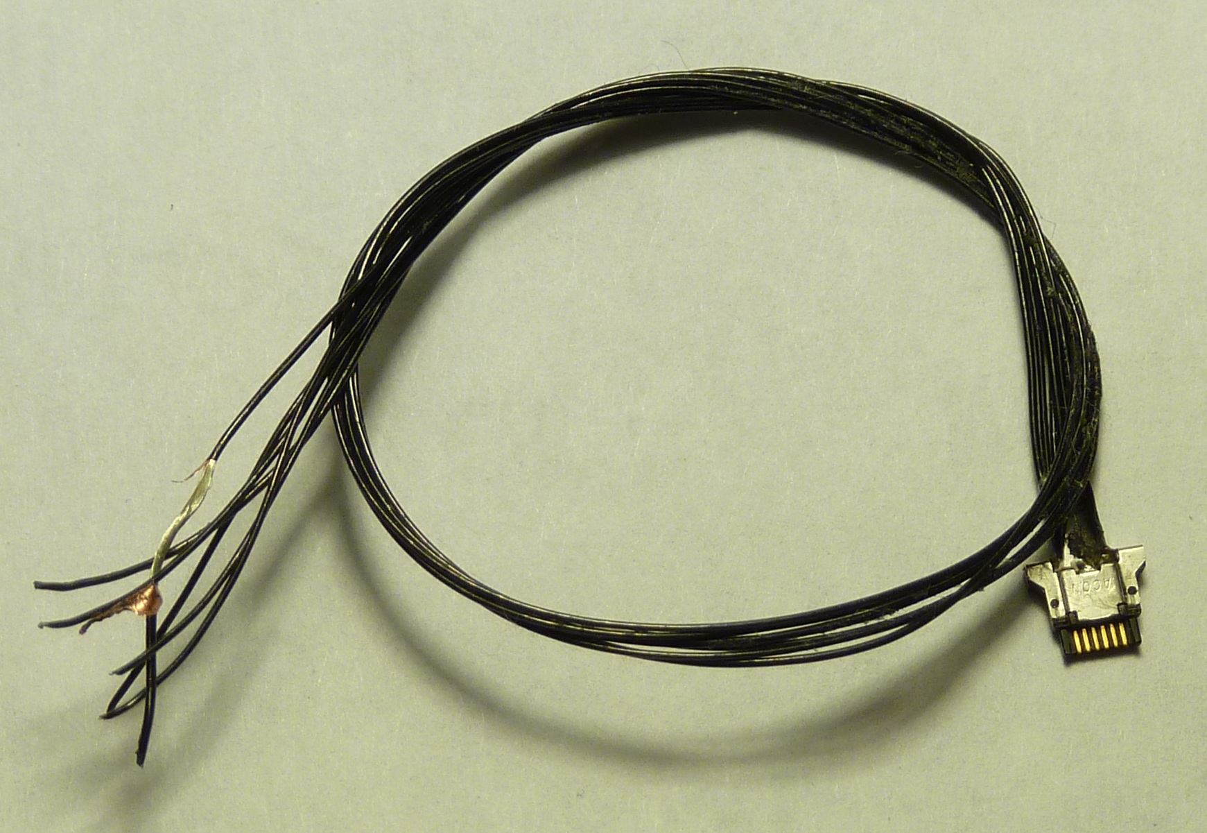
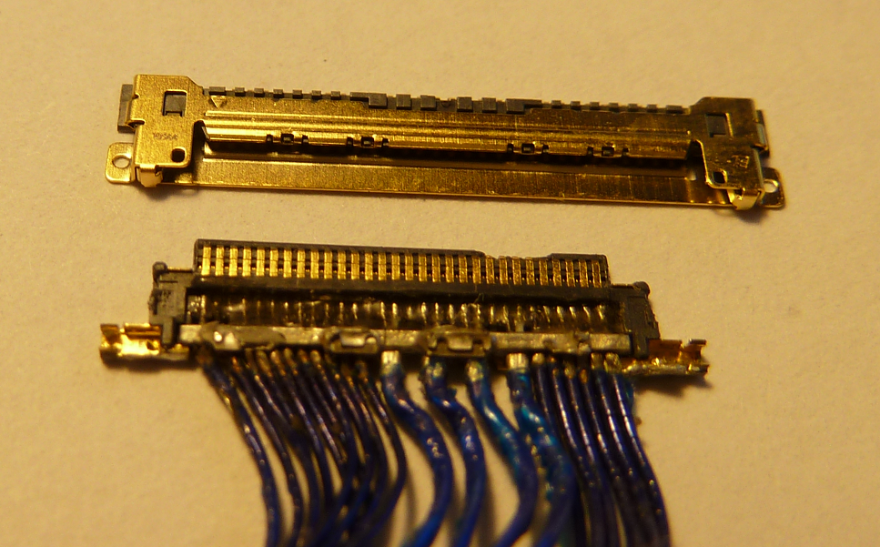
A shipment of components including the connectors intended for the Macbook LCD breakout board arrived yesterday. I-PEX components are not carried at the usual US distributors, so I opted to order a TE part that a random source seemed to indicate might mate (5-2069716-2). Well…

Well that isn’t going to work.
That’ll teach me for not doing my research. The pin pitch isn’t even correct. So I cost myself a few bucks and a week of time. Damn it all. But I have ordered a few genuine I-PEX Cabline-CA connectors on eBay, so in only another two weeks, I should have things figured out enough to spin a “proper” simple breakout. The long leadtime of OSH Park is really killing me these days.
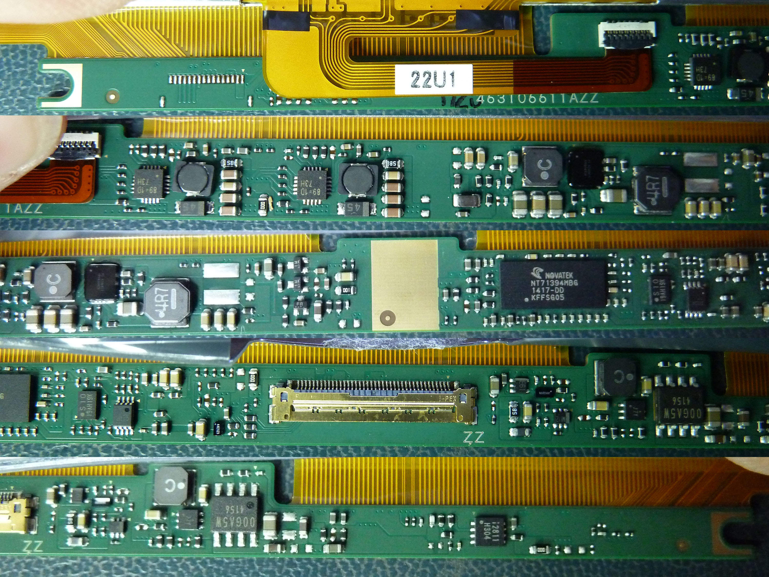
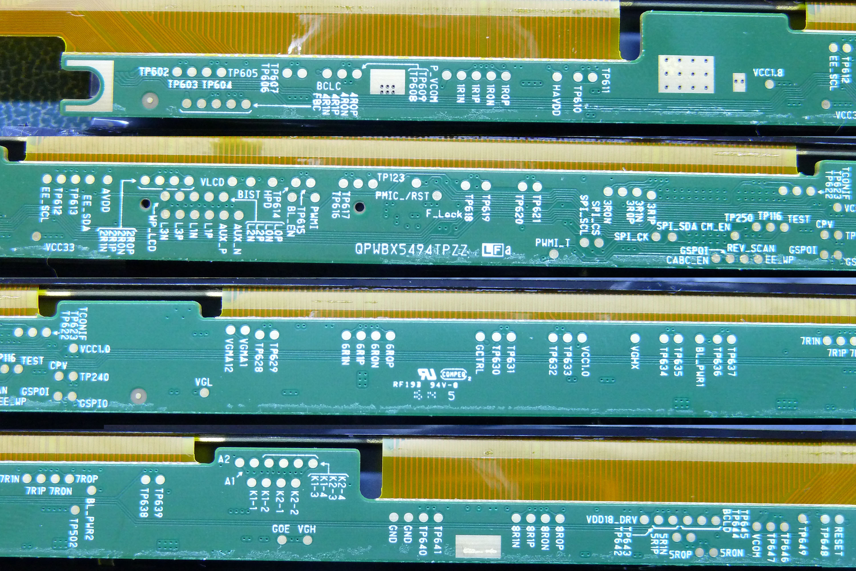
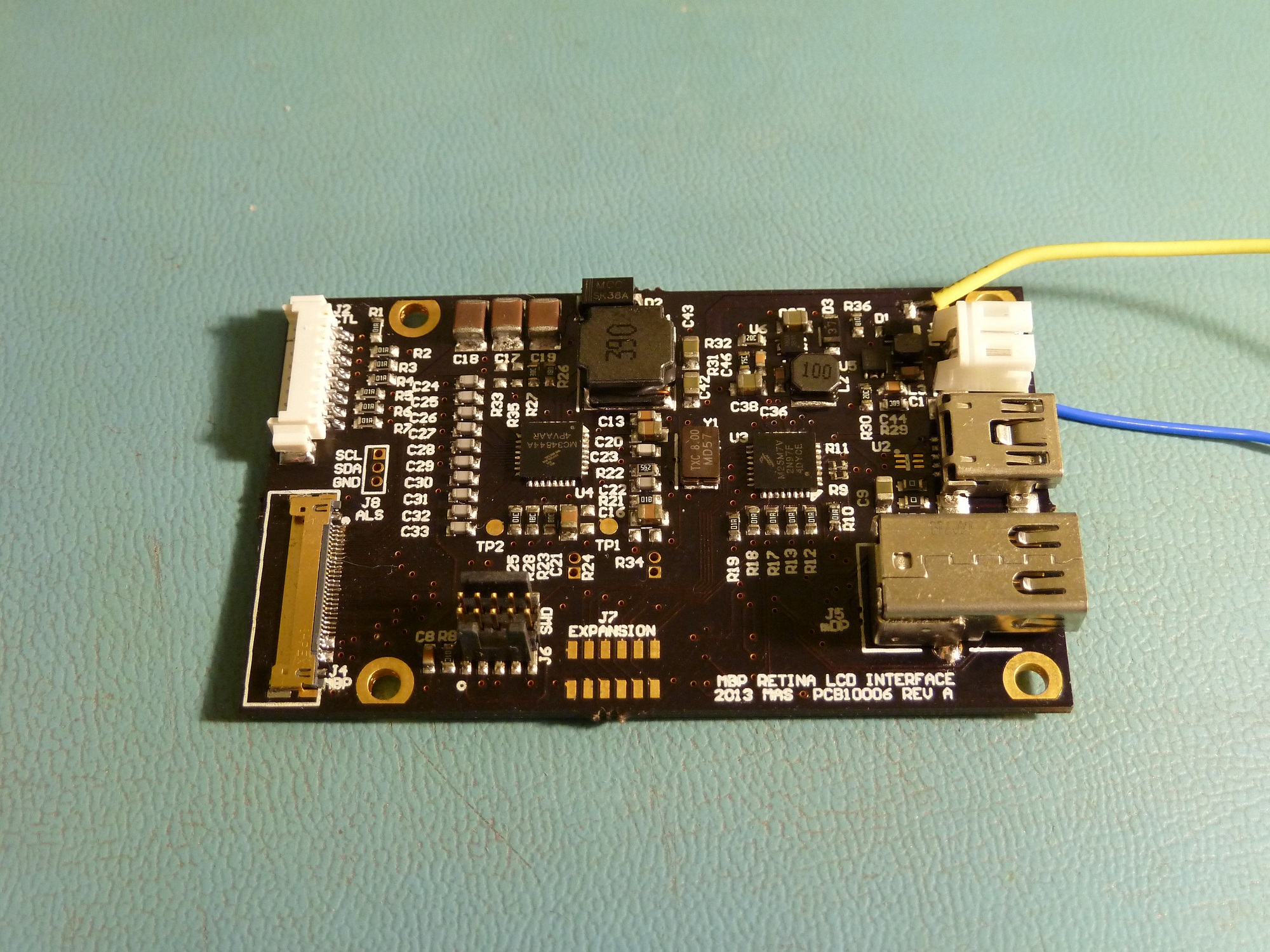
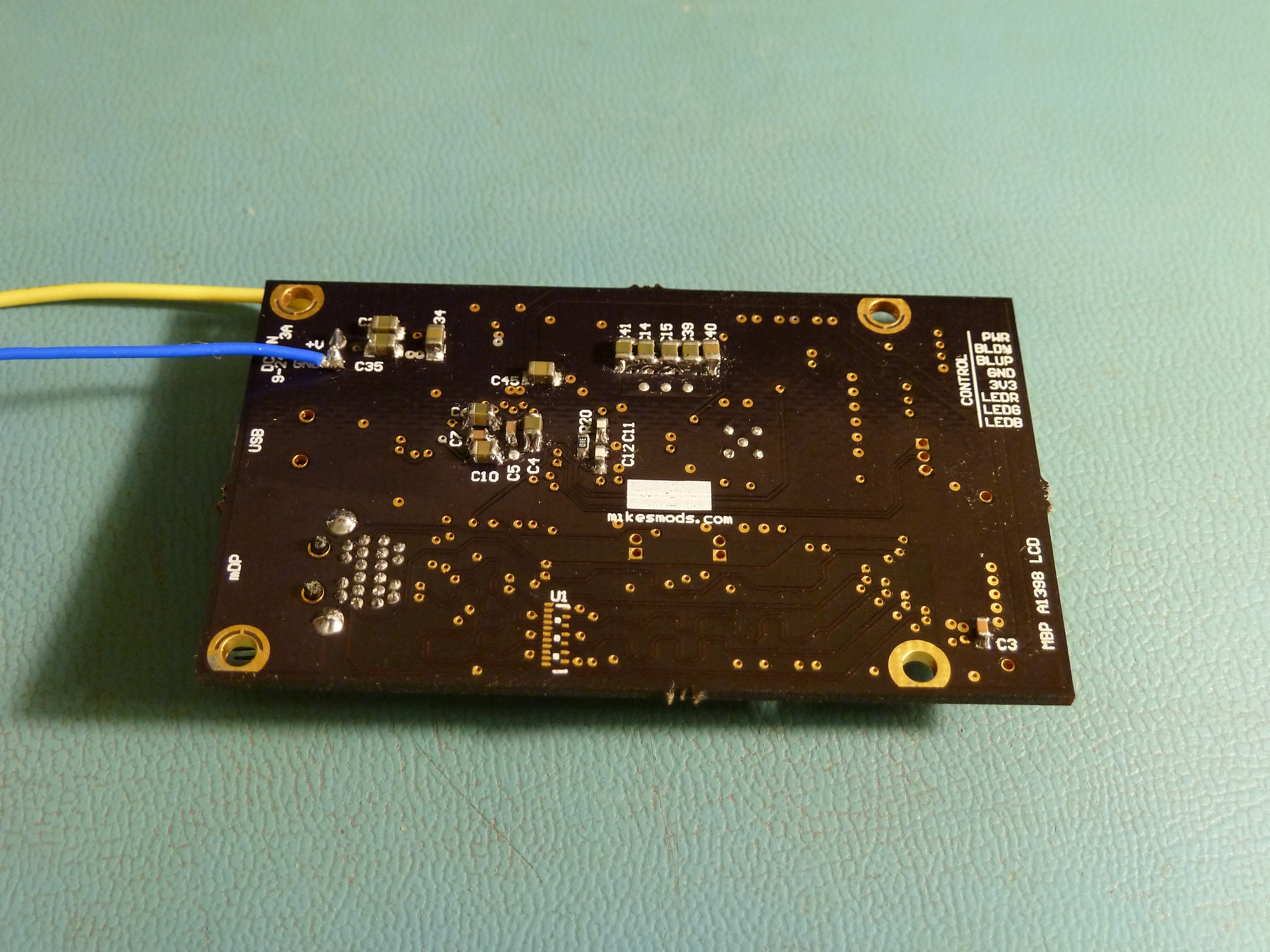
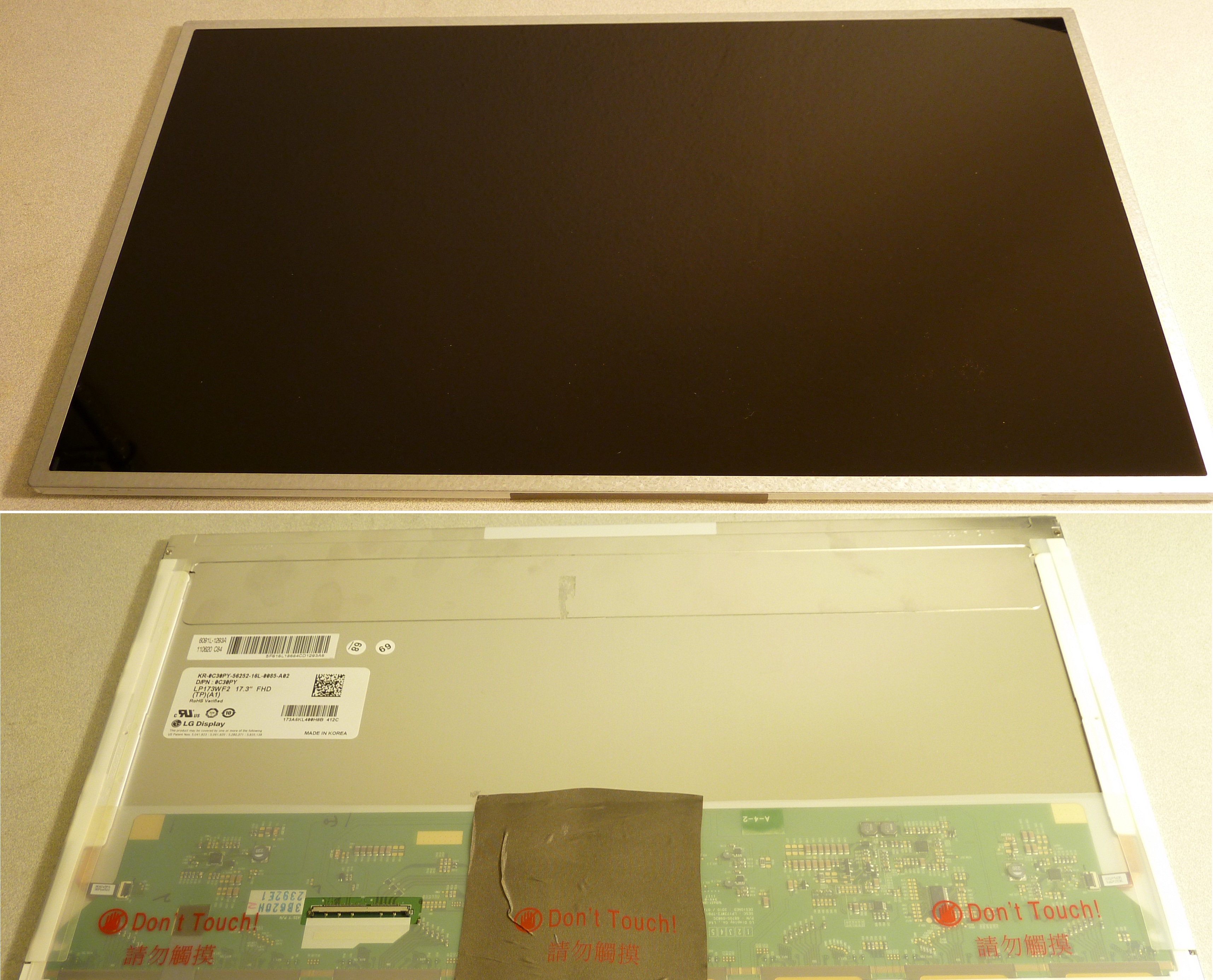
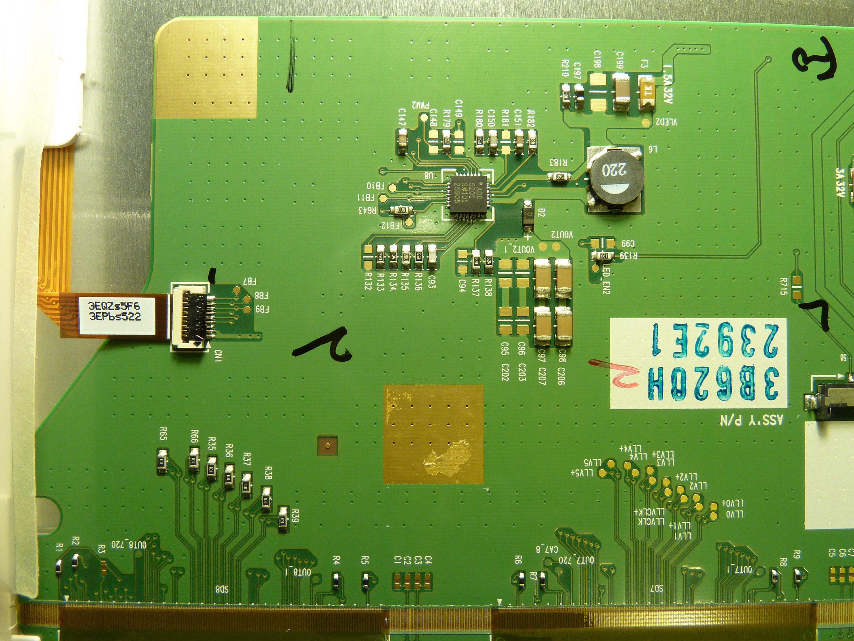
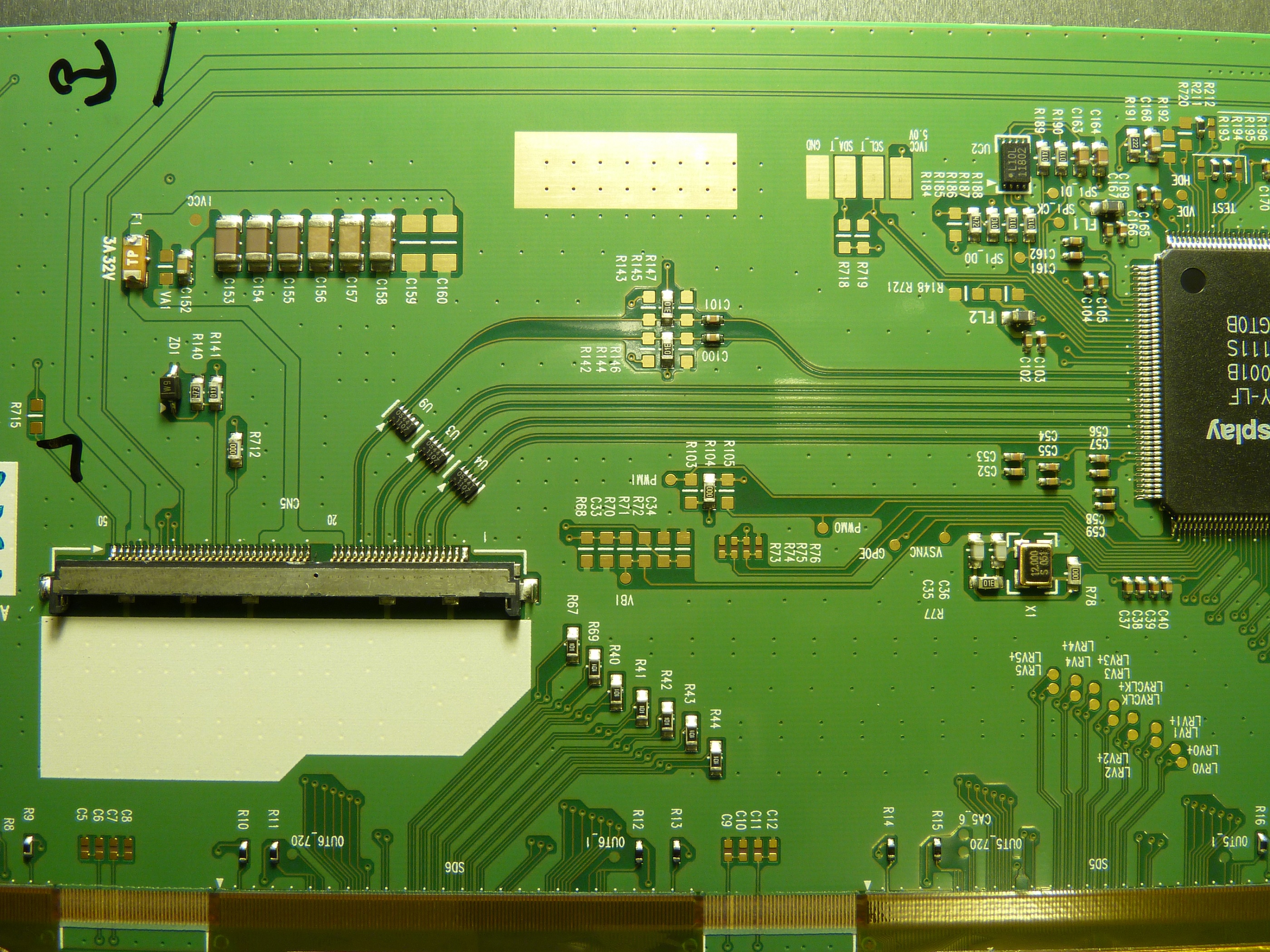
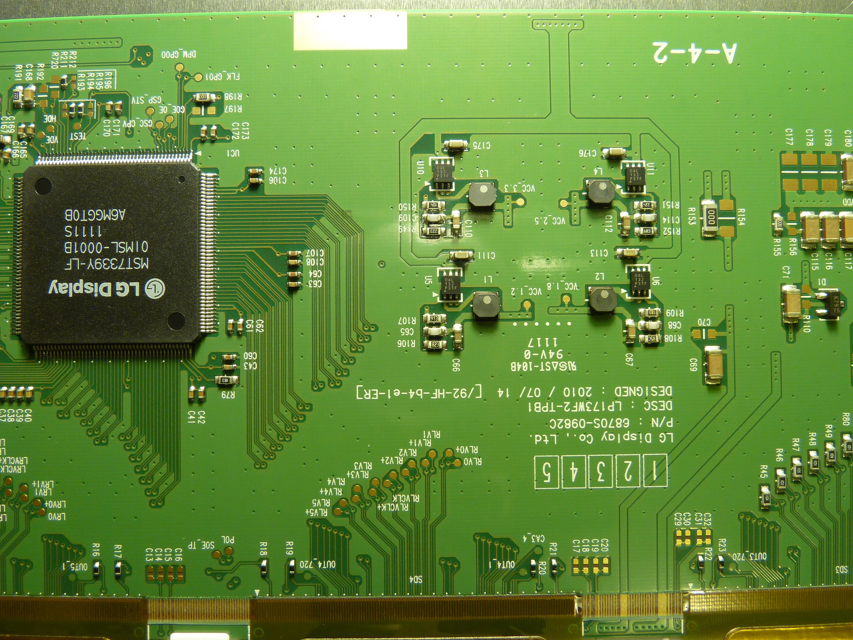
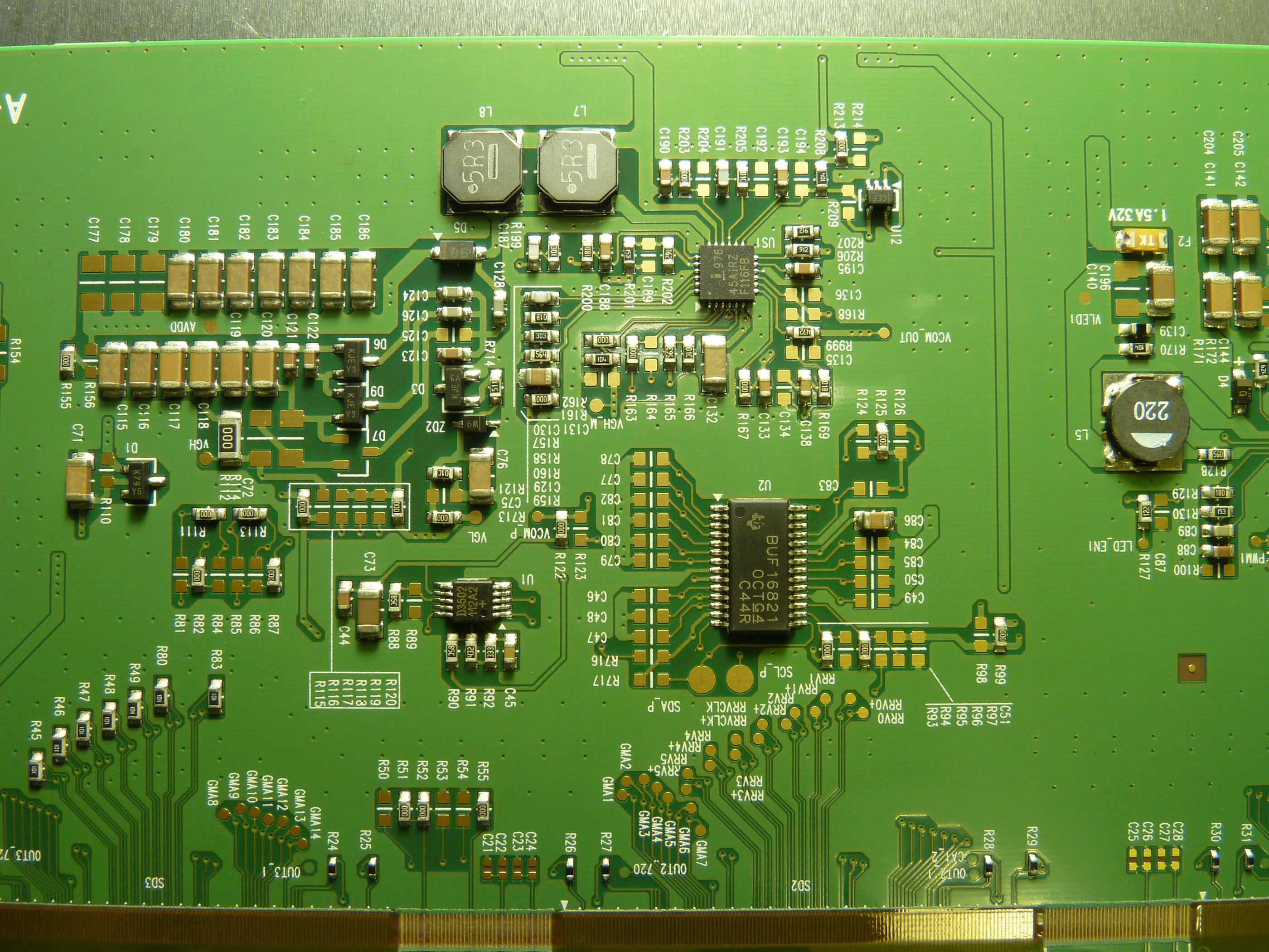
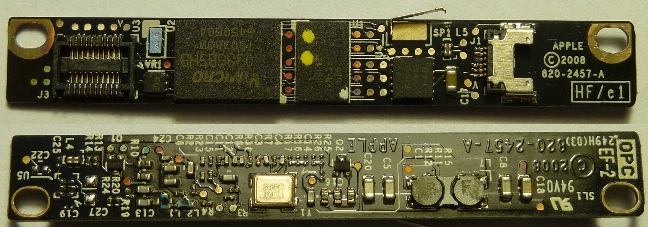
In the meantime, Daniel has sent me some more photos of his Samsung controller boards and has made great progress in his efforts. The Samsung boards look like this:
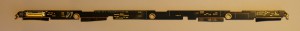
Macbook Retina controller board, Samsung version – component side
Macbook Retina controller board, Samsung version – connector side
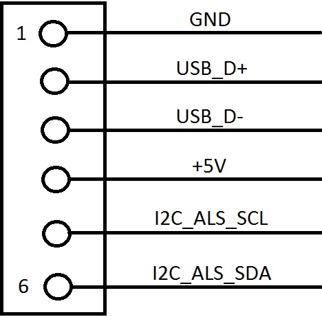
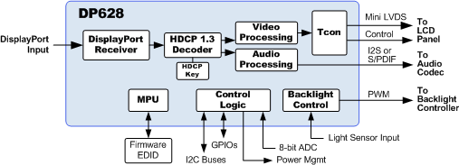
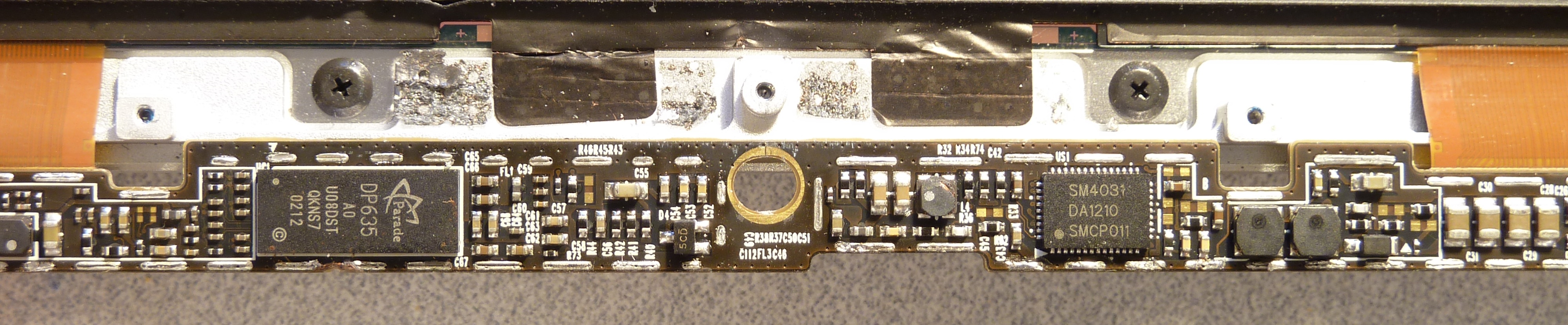
His progress has compelled me to do a little additional work of my own – even though I swore I wouldn’t solder more jumpers to the panel. Oh well, promises were meant to be broken. In order to know where to stick wires, I have spent some time investigating the hardware that makes up the controller PCB. The brain of the display is the ParadeTech DP635 LCD timing controller. While the specification for this part is not freely available, ParadeTech sells several other Tcons, such as the DP628. Here is a block diagram of the innards of that part:
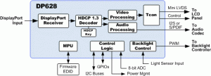
Block diagram for the ParadeTech DP628 DP Tcon.
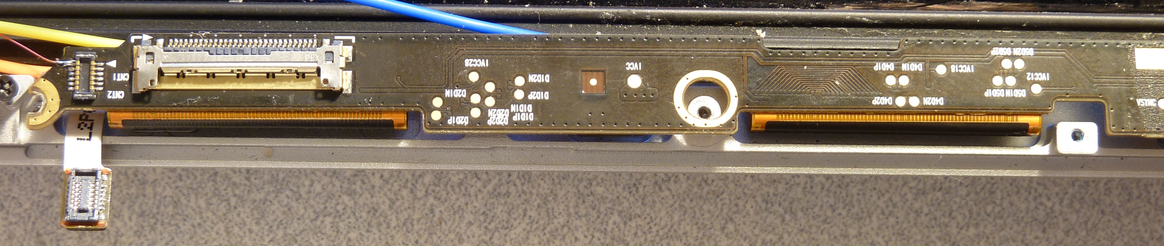
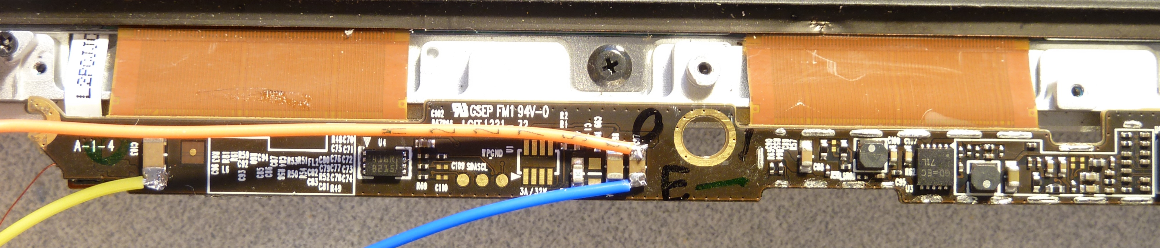
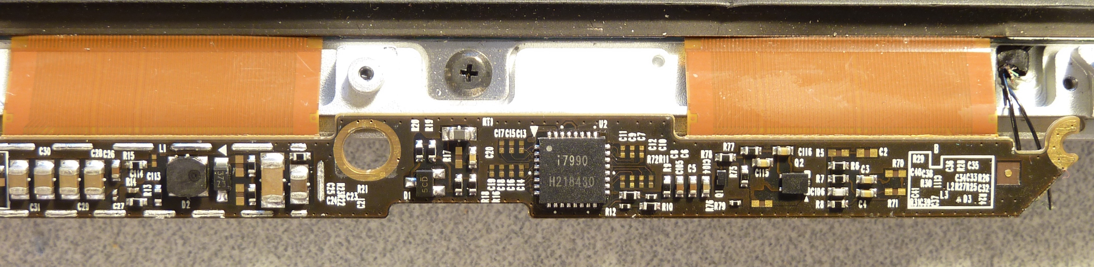
We will assume that the DP635 works sorta-similar. From this, we can deduce that this IC takes in the DisplayPort signal and spits out something compatible with the chip-on-glass driver ICs on the panel. In the ‘628 this is miniLVDS, and it’s reasonable to guess that this may be similar to the way it is done in the ‘635. The backside of the controller PCB has pairs of testpoints labeled D1D1P/D1D1N, D1D2P/D1D2N through D9D1P/D9D1N, D9D2P/D9D2N, nine pairs of pairs in all. Presumably this is eighteen differential pairs carrying the decoded video data as converted from the DisplayPort source. As my panels are functional I will leave this as a theory and not pull off the IC to probe it out to the testpoints.
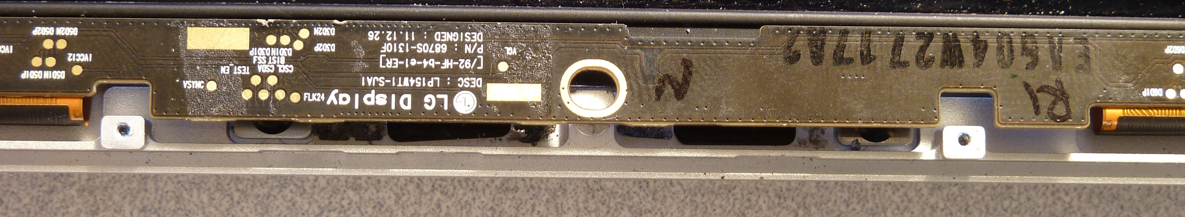
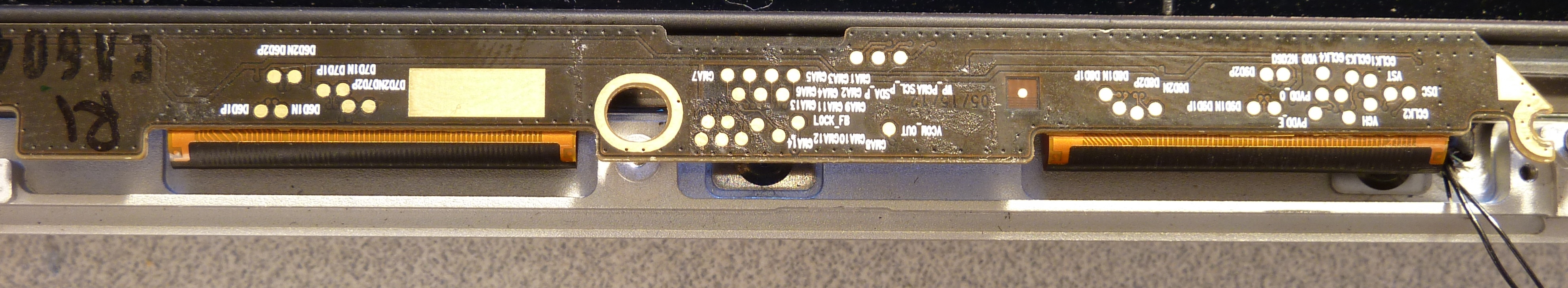
Speaking of testpoints, there are plenty of them. Here’s a list of the marked points, primarily found on the connector side of the PCB:
- D1D1P/D1D1N, D1D2P/D1D2N thru D9D1P/D9D1N, D9D2P/D9D2N (differential video channels, as noted above)
- IVCC
- IVCC28
- IVCC18
- IVCC12
- VSYNC
- CSCL
- CSDA
- TEST_EN
- BIST
- FSS
- FLK24
- VGL
- GMA1 thru GMA14
- LOCK_FB
- VCOM_OUT
- WP_PGMA
- SCL_P
- SDA_P
- PVDD_O
- PVDD_E
- GCLK1 thru GCLK4
- VDD
- VST
- DSC
- VGH
- SDA, SCL, WP_GND (near the EEPROM on the component side)
Some of these pins seem to be pretty self-explanatory (SDA/SCL/WP, for instance). Also, the “IVCC” pins are obvious. These pins indicate that there should be a 2.8V, a 1.8V, and a 1.2V rail. Probing these pins did not immediately yield these results, which merits discussion.
In the previous post, I applied 3V to the panel, which I figured would be enough to activate the switching power supplies on it whether they were meant to run on 2.5V or 3.3V (the latter being extremely common, and the former starting to gain traction in newer panels). It was unusual to find the panel fading to white. Per the eDP specification, the panel should be continuously refreshed to black with no signal driving it, so something seemed to be wrong.
There appear to be around a half dozen voltage rails on this board. Testpoints break out input voltage (point IVCC) as well as 2.8V (IVCC28), 1.8V (IVCC18), 1.2V (IVCC12), -6V (PVDD_O and PVDD_E) and 20V (VGH) (more on those two some other time). But the 1.2V and 2.8V testpoints appeared inactive. Both of these supplies appeared to be driven by mystery-chip GD=EC on top. Thus, my immediate theory became that the DP635 relies on the 2.8V and/or 1.2V rail, and the fading to white is the (powered) LCD glass resetting as it is not being actively driven to black. Why white I don’t quite understand yet since IPS is naturally black, but let’s ignore that for now. I increased my input voltage to 3.3V at this point, which seemed to make no difference.
I began to suspect that GD=EC is a dual buck regulator, based on the testpoints underneath it and the general layout of the components. I probed the components and ended up with a schematic that appeared to agree. I noted before that I suspected the part was a Richtek regulator, which came to me when I found a teardown of another product which had a confirmed Richtek part with a similar marking. Now armed with the fact that the part is a dual buck regulator, and that it comes in a 10-pin 3×3 DFN, this was enough to track it down – the part is a Richtek RT8035 (Datasheet).
From the datasheet’s pinout (which I had already mostly figured out from probing the surrounding components), I located the device’s Enable pins and noted that the voltage measured here with 3.3V provided by the source was around 1V, which according to the regulator datasheet is between the Enable and Disable voltage limits, which puts it somewhere in a possibly-undefined region of operation. In fact, probing the outputs of the regulator showed that there were occasional pulses of voltage produced.
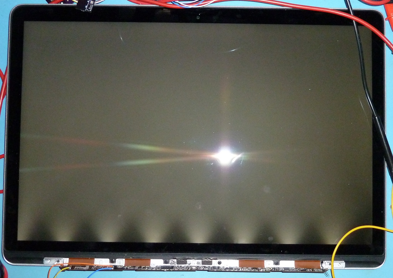
Well, if it was a 2.5V panel it wouldn’t have these problems at this voltage, so that idea was discarded. If this is indeed a 3.3V panel, it should be safe to apply up to 3.6V or so. So I applied 3.5V to the panel, and lo and behold, the panel turned black, the current draw increased, and upon testing all the supplies appeared to be online.
I did a little more investigation, since that seemed a strange operating voltage, and noted that I was actually losing quite a lot in my wiring. Even the two feet of 22AWG I was using was dropping one or two tenths of a volt. When compensated for that, the panel seemed to run on 3.3V – but only just barely. It is hard to believe that it is actually a 3.3V panel, it seems to have almost no bottom-end voltage tolerance. My rational side says the panel should easily run on something higher than 3.3 – maybe 5? – since all of its important circuitry appears to be powered on switching subregulators and not from the incoming VCC. But I can’t bring myself to smoke an otherwise working panel, so for now I will set my supplies to 3.5V and call it good. Plus DisplayPort runs on 3.3V and the pullups and pulldowns might use the input rail, so we don’t want to go too high. For what it’s worth I have not seen any other Apple LCD product use a logic rail above 3.3V – not to say that it isn’t the case, but it would be uncommon.
So now the panel was running, drawing about 600mA at 3.3V (for what it’s worth, it only drew about 200mA when it was misbehaving and showing only white). That’s about 2W of panel drive power, which sounds about right. It might rise slightly when driven under certain circumstances. Neat! Let’s do something with it.
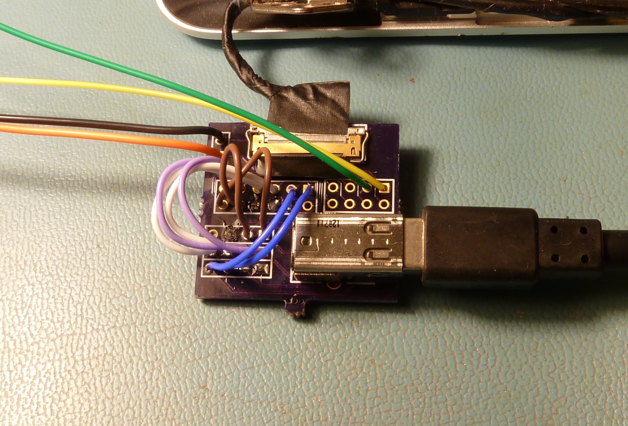
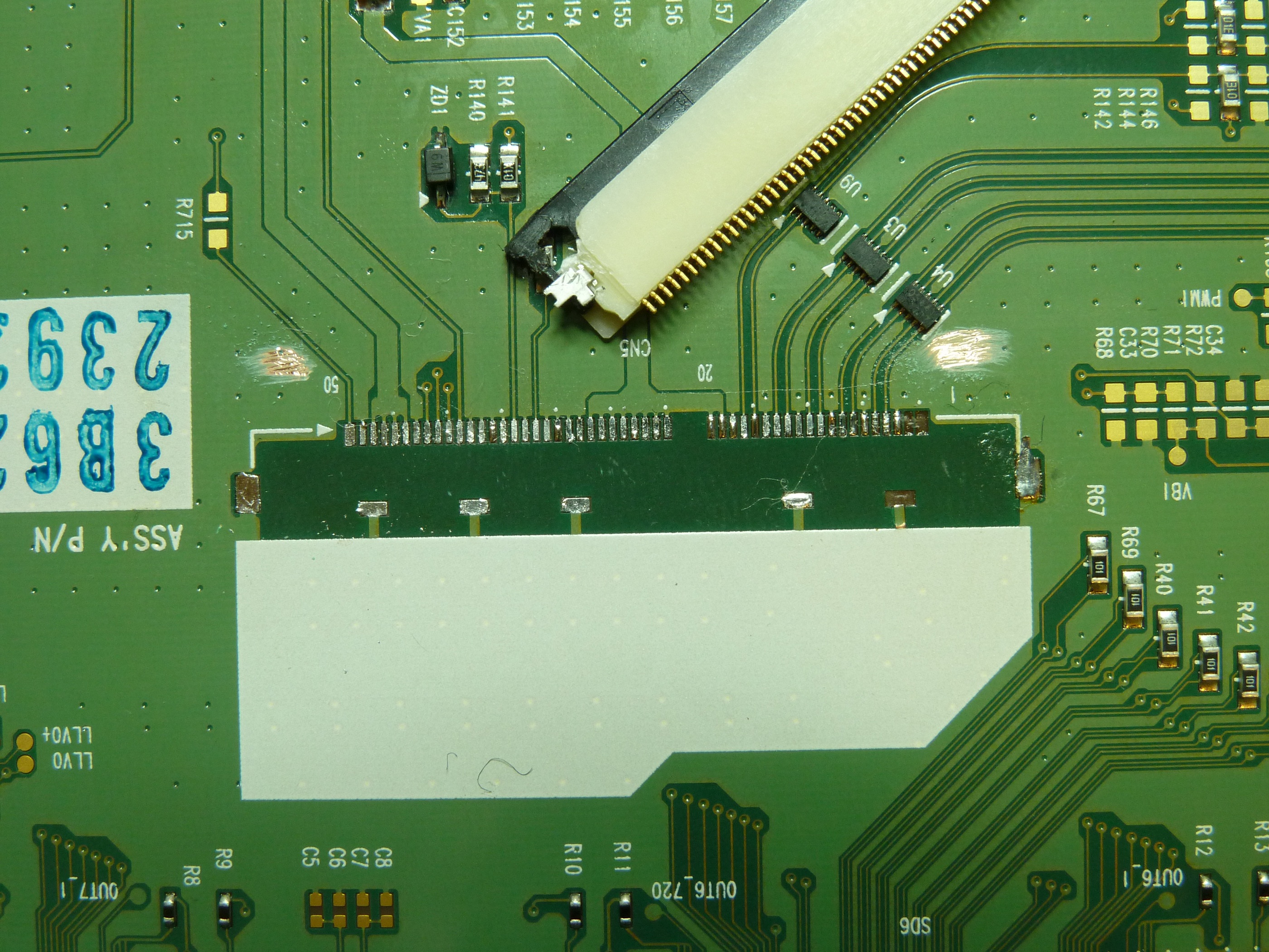
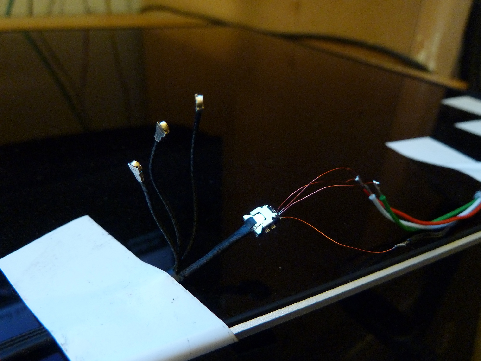
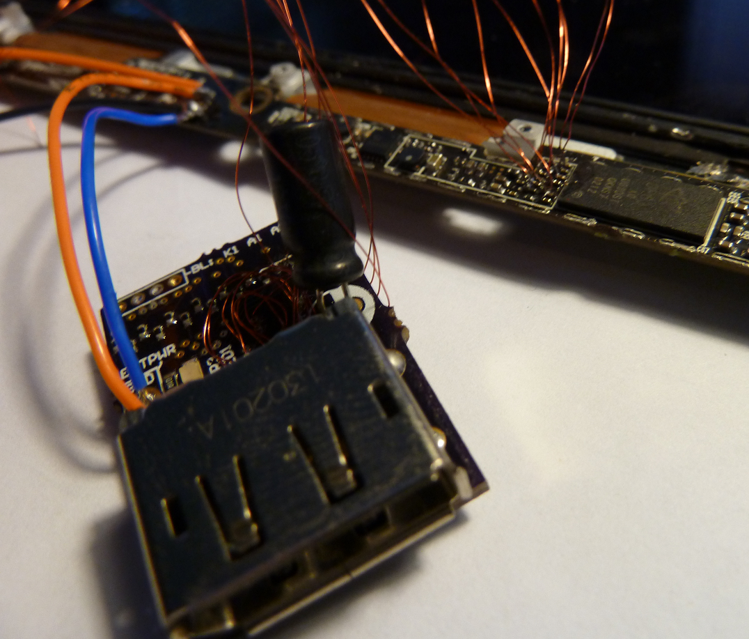
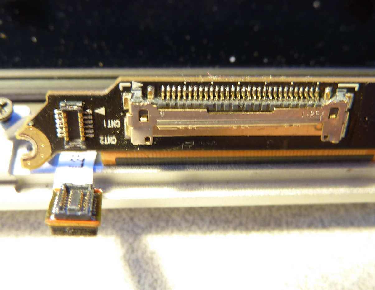
To go any farther, I’d have liked to use a breakout cable to avoid having to solder to the panel itself. But what the hell, I’d already soldered on it a ton to remove the shields and to install some power and test jumpers, so what had I to lose. Assuming from the block diagram of the DP628 (remember that? I’ve rambled a lot since then!) that the DP635 takes in DisplayPort, and remembering from the DisplayPort specification that the DP lanes and AUX pins are capacitively coupled, and additionally that AUX and HPD have pullup or pulldown requirements, there will need to be a group of capacitors and resistors somewhere on the board that correspond to the requirements of the specification. Suspiciously, next to the DP635 appears this formation of components:
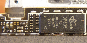
Ten capacitors and a handful of resistors, right next to the Tcon? Iiiiinteresting.
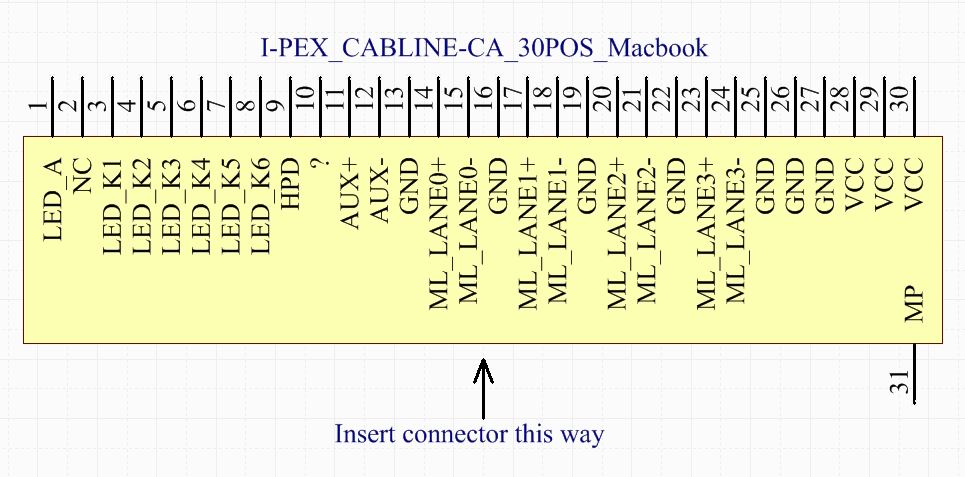
The reference designators for these parts are listed off to the side – from top to bottom, left then right, the components are R47, R48, C75, C76, C77, C78, R49, then C69, C70, C71, C72, C73, and C74. These are seriously small 0201 parts. I noted in the last part of this writeup that I’d located the DisplayPort lane pins on the connector. To confirm that these components are related to DisplayPort, I probed for continuity between here and the connector, and indeed they appear to be. What’s more, R47 and R48 are 1Mohm resistors connected to capacitors C69 and C70; one resistor pulls to GND and one to VCC. This precisely matches the description of the AUX channel. Probing the center of the the series set, we can finally confirm that pin 11 on the I-PEX is AUX+, while pin 12 is AUX-. Continuing in order, pin 14 connects to C71, pin 15 to C72, pin 17 to C75, pin 18 to C76, pin 20 to C77, pin 21 to C78, pin 23 to C73, and pin 24 to C74. We still don’t know what order the lanes are in, but at least now we know the correct connection for AUX.
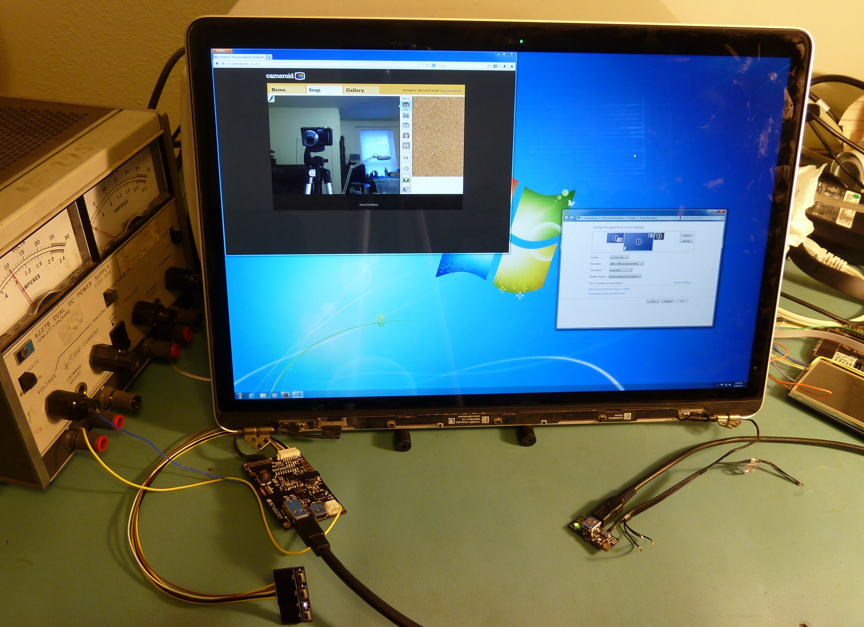
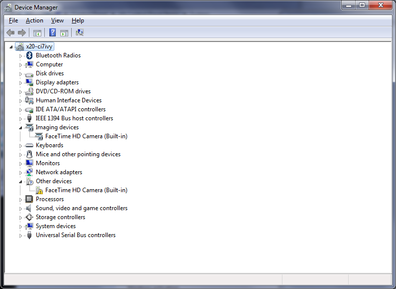
The advantage of knowing AUX is that now we can start connecting the panel to a PC and can see what Windows thinks of it. By wiring the panel to a prototype of my Simple iPad Breakout (only for the DisplayPort connector) and shorting HPD to VCC, I got the panel to register as a 2880×1800 “Color LCD”:
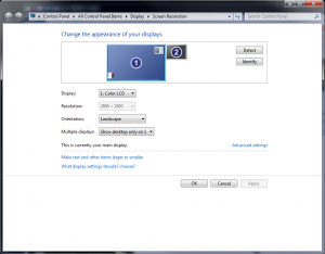
This is how the Macbook Pro Retina LCD registers to Windows. This is a screenshot; the panel doesn’t actually work yet since I don’t have the lanes connected.
Hooray, it’s alive! When I was dealing with the white-screen issue I wondered if the damage to the PCB visible next to the DP635 had rendered the panel an expensive paperweight. Now the effort is only figuring out the ordering of the lanes and the location of HPD, both issues which would be simple with a breakout. For HPD, we need only measure which of the remaining unknown pins (9 and 10) goes logic high when voltage is applied. For the lane ordering, there are only four probable orderings (0-/0+…3-/3+, 0+/0-…3+/3-, 3-/3+…0-/0+, 3+/3-…0+/0-), and with a breakout and jumper wires this should be found very quickly.
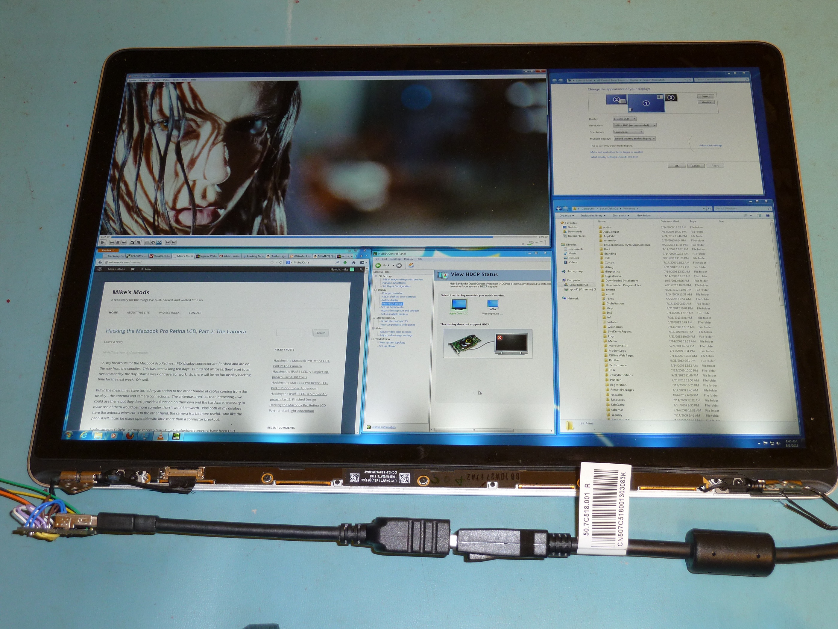
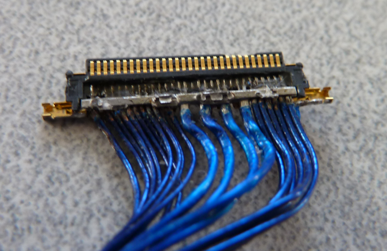
I got impatient and soldered in 36AWG magnet wire jumpers on all the lane lines, and tried a couple of the arrangements but have not yet been lucky enough to land on the correct one. I’m not sure I’ll continue with this though – it’s massively frustrating, and I’m not even sure this panel is operational nor whether my soldering to the tiny capacitors makes a good connection. It will take another two weeks, but I think I’ll just wait until I get in the corrected breakout boards to continue down this path.

This was absolutely no fun to solder.
In the meantime I have been working on the backlight driver for the panel. For the iPad panel, I used a Linear Technology LT3754 16-channel driver with integrated boost supply. I like the concept of using drivers with internal boost supplies – one less IC to buy, and a decent savings of board area. When you bump up from seven to sixteen series LEDs, the number of drivers that are capable of boosting to the necessary 51V or so internally is not quite so large. The ‘3754 and its max 45V output is no longer usable.
I think for this panel I will be investigating the Freescale MC34844A. This part is a 10-channel, 60V, 80mA/channel driver which can modulate based on analog input, PWM, or (interestingly) an I2C interface. There exists a simpler 6-channel version of this chip, the MC34845, and I briefly considered using it, but despite the nicety of being a slightly simpler chip, the ’45 is Not Recommended for New Designs (is going end of life soon) so I dare not use it. The only real downside of the MC34844A is that it only supports up to 28V input. I’m a big proponent of hugely overdesigned voltage input overhead, because people do terrible things to electronics sometimes, and I liked the fact that the 3754 could work all the way up to 40V “just in case”. So this version will only work to 24V, oh well. I suspect most people would run it on 12V anyway so maybe I am needlessly cautious. I already have parts for the new backlight driver, so as soon as I spin a board for it I can try everything out.
Holy cow, that’s a lot of words that don’t really have a lot of useful content. I’m really feeling a setback since I built the first breakout around an incorrect connector. But I’ve got the correct board in the works, and will order it on Monday, and hopefully by mid two weeks from now I’ll have a proper board and will have the panel running. At least that’s the grand plan – I don’t guarantee I won’t screw up again… it’s a good thing OSH Park is so cheap!
In the meantime, off to work on the iPhone 4 LCD… stay tuned for that in a later episode.
<< Previous post in this series … Next post in this series >>