I’m a huge sucker when it comes to playing with shiny new tech, and straight from the shiny tech factory I’ve gotten ahold of a new toy which in terms of raw number of pixels puts the previous panels I’ve been working with to shame. Say hello to the Sharp LQ156D1JX01!

It’s pretty glossy. Look, a reflection of some of my test equipment!
The LQ156D1JX01 is a new inductee to the ultra-high-DPI panel club, whose members have lately found their way into many high-end gaming laptops and ultrabooks. This particular panel is a pull from a Toshiba Satellite P50T. The panel measures a whopping 3840×2160 pixels (that’s 4K, or 8.29 megapixels!) in a mere 15.6 inch size. Now, that doesn’t quite compare to the current generation of cell phones with 5-inch 4K screens, but at something like 282PPI it’s nothing to scoff at either. This pushes far above the 220PPI of the Macbook Pro Retina panel that we’ve played with before, and puts it somewhere between the 264PPI of the iPad 3 Retina panel and the 324PPI of the iPad Mini 2 Retina. Like the Macbook and the iPad, the LQ156D1JX01 runs on 4-lane Embedded DisplayPort. Where it differs a bit is that this panel is reportedly addressed as two 1920×2160 half-displays over DisplayPort 1.2’s Multi-Stream Transport. This may have been done to simplify timing requirements for such a massive display.
I don’t happen to have a proper connector on hand for this panel so I haven’t fired it up yet, but like any good engineer, before even bothering to plug in my new toy I went ahead and tore it apart. This was actually a necessary step, because there is currently no publicly-available datasheet for this panel, so we need to figure out the pinout of the connector in order to make it do anything anyway.
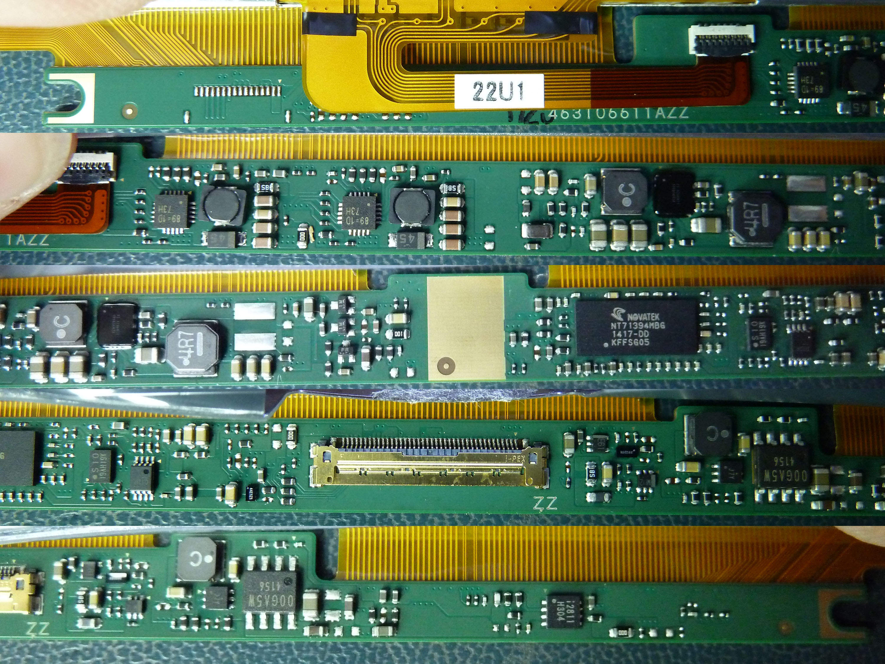
LQ156D1JX01 control PCB top side collage
Before delving into the pinout, we can find out several things about this panel by looking at the design of the control board. The main connector is made by Dai-ichi Seiko I-PEX and appears to be a 40-position CABLINE-CA series part, possibly 20525-040E-02 (pdf link). The panel is driven by a Novatek NT71394MBG. This part does not seem to have any publicly available information, but we’ll assume it’s a timing controller ASIC. There is a TI power management IC that appears to generate all the necessary panel voltages; I think it’s a TPS65642A (pdf link). There are also two chips marked 89=1D, these are Richtek RT8532 boost LED drivers (pdf link). The design of the backlight flex implies that each of these ICs drives four LED channels, despite being capable of six.
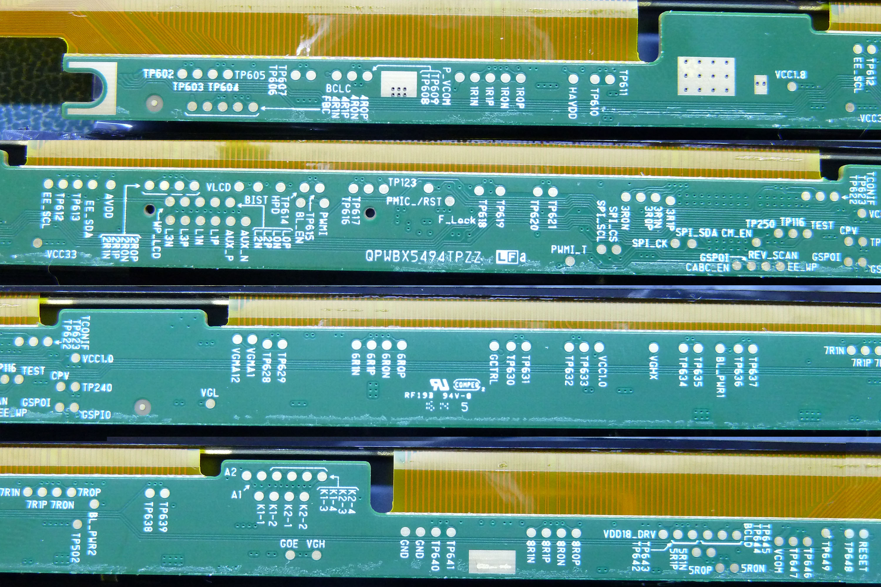
LQ156D1JX01 control PCB bottom side collage
Now that we have some idea of what’s going on in the panel, on to the pinout. Thanks to Sharp, this task is simple, because all of the pins are connected to convenient labeled testpoints on the bottom of the board. I haven’t tested the panel yet so I don’t know if this is 100% accurate, but as far as I can tell at this point, the pinout for the LQ156D1JX01 is as follows:
| Pin | Name | Description |
|---|---|---|
| 1 | PMIC_/RST | Power Management Reset, Active Low |
| 2 | GND | Ground (Shield) |
| 3 | L3N | Embedded DisplayPort Lane 3 Negative |
| 4 | L3P | Embedded DisplayPort Lane 3 Positive |
| 5 | GND | Ground (Shield) |
| 6 | L2N | Embedded DisplayPort Lane 2 Negative |
| 7 | L2P | Embedded DisplayPort Lane 2 Positive |
| 8 | GND | Ground (Shield) |
| 9 | L1N | Embedded DisplayPort Lane 1 Negative |
| 10 | L1P | Embedded DisplayPort Lane 1 Positive |
| 11 | GND | Ground (Shield) |
| 12 | L0N | Embedded DisplayPort Lane 0 Negative |
| 13 | L0P | Embedded DisplayPort Lane 0 Positive |
| 14 | GND | Ground (Shield) |
| 15 | AUX_P | Embedded DisplayPort Aux Channel Positive |
| 16 | AUX_N | Embedded DisplayPort Aux Channel Negative |
| 17 | GND | Ground (Shield) |
| 18 | VLCD | 3.3V LCD Power |
| 19 | VLCD | 3.3V LCD Power |
| 20 | VLCD | 3.3V LCD Power |
| 21 | VLCD | 3.3V LCD Power |
| 22 | BIST | Built In Self Test |
| 23 | GND | Ground (LCD Power) |
| 24 | GND | Ground (LCD Power) |
| 25 | GND | Ground (LCD Power) |
| 26 | GND | Ground (LCD Power) |
| 27 | HPD | Embedded DisplayPort Hot Plug Detect |
| 28 | GND | Ground (Backlight) |
| 29 | GND | Ground (Backlight) |
| 30 | GND | Ground (Backlight) |
| 31 | GND | Ground (Backlight) |
| 32 | BL_EN | Backlight Enable |
| 33 | PWMI | Backlight PWM |
| 34 | EE_SCL | EEPROM Clock (EDID?) |
| 35 | EE_SDA | EEPROM Data (EDID?) |
| 36 | BL_PWR1 | Backlight Power |
| 37 | BL_PWR1 | Backlight Power |
| 38 | BL_PWR1 | Backlight Power |
| 39 | BL_PWR1 | Backlight Power |
| 40 | WP_LCD | Write Protect? |
I have not marked the backlight voltage in the table, because I am not certain what the design voltage range is. RT8532 has an operating range from about 5V to 24V, but it is not currently known what the components in the display are actually rated for. My guess is it’s probably safe up to at least 12V, but try at your own risk.
It’s interesting to see EEPROM pins brought out. I suspect these are for the EDID EEPROM, maybe for factory programming of the device. Or maybe it’s something completely different. Again, without having fired up the panel, this is all speculation. There is an explicit “EE_WP” testpoint which is not the same as the “WP_LCD” that is brought out; I don’t have any good idea for what the latter may be used for.
So that’s about it. The next step is to wire up a connector and get the panel running, but that won’t happen today. Stay tuned for a followup post.