Hello again, and my apologies for the long time since the last one. Today I’ve got a quick topic to discuss, and although it’s fairly obvious, I don’t think it’s documented elsewhere online.
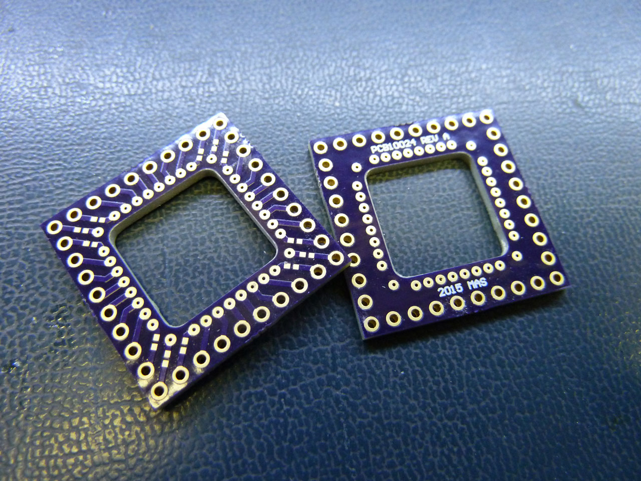
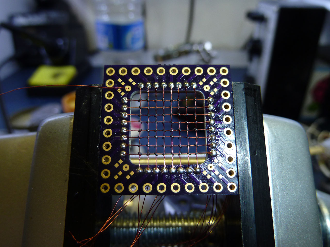
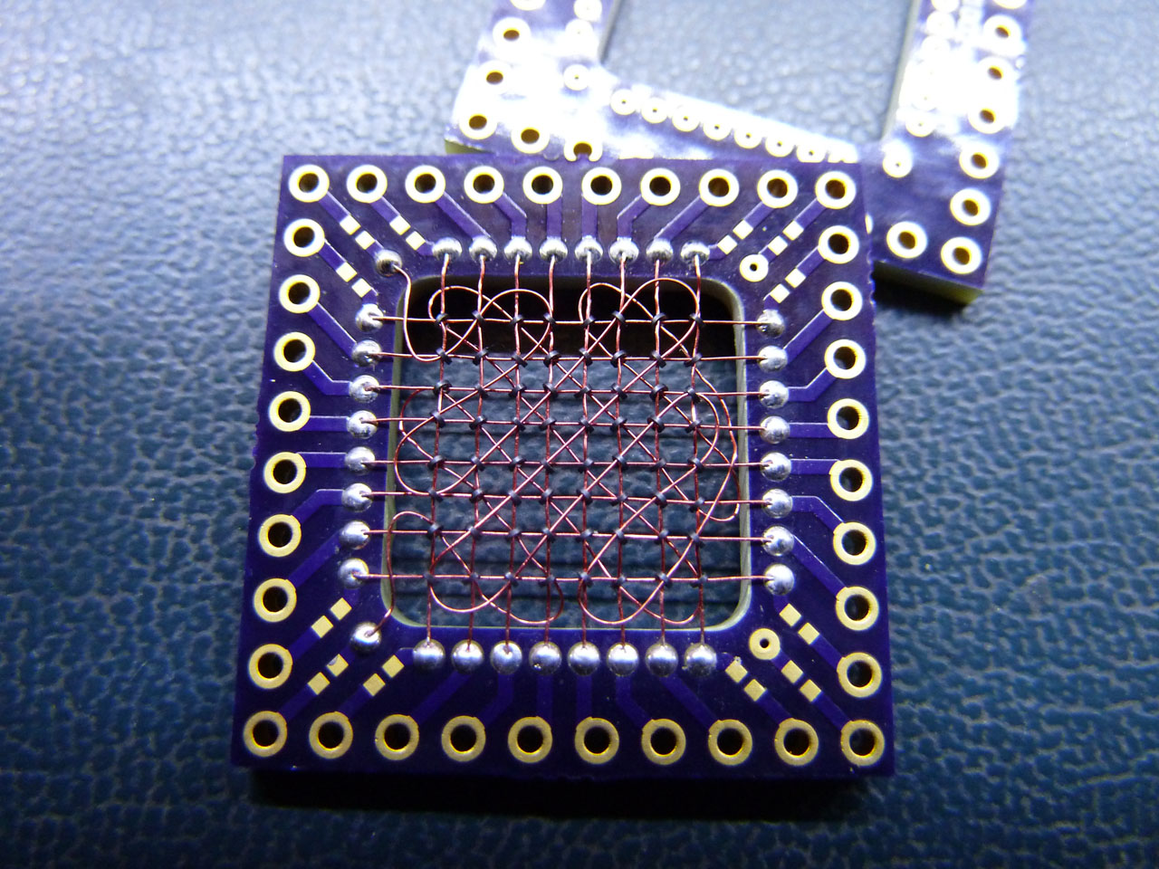
I’m working on a project for which I’ll be building a fairly sizable core memory array (see here for the first post on this topic, which covers the construction of a small demonstration array). As noted in the original post, it is simple to address a huge number of cores in an array because the core material will only change magnetic state when a sufficiently large current is passed through it; any smaller current will leave the core in its initial state. Thus, by passing only half the necessary state change current through the core through each of two wires, and by ensuring that no two cores have the same two wires passing through them, any individual core may be selectively read from or written to based on the set of wires that are energized.
But how much current is necessary? There is no standard (to my knowledge) that says all memory cores require x milliamps to flip. If you buy a set of random cores on eBay like I did, this is a question that needs to be answered before any further design work can take place. So I tried a few methods, found some things that worked and some things that didn’t work so well, and decided to share my results.
First, recall from Ampère’s Law that a current flowing in a wire creates a circular magnetic field around that wire. If the wire were pointing toward you and the current flow was coming toward you, the magnetic field would be counterclockwise – or using the common “right-hand rule”, if you wrap your right hand around the wire with your thumb pointing in the direction of the current flow, your remaining fingers determine the direction of the field. From the right-hand rule we can also see that if we want the magnetic field to reverse – which we need in order to change the data on the core or to read out the data that is there – we would have to flip the flow of current so it goes the other direction.
So, I soldered a 51 ohm resistor across both ends of a piece of 36AWG magnet wire with a core threaded onto it, and then soldered one 150 ohm resistor to each end of a second piece of magnet wire which was also threaded through the core. Note that neither of these values were calculated nor should be critical. I connected an oscilloscope probe across the 51 ohm resistor, then connected the 150 ohm resistors to a handheld digital multimeter (on Current mode), then to a bench power supply and applied a few volts. I then tried swapping the leads on the power supply to change the direction of the current, and watched the oscilloscope. No matter how many times I swapped the leads, or what voltage I applied, I never got anything that resembled the clean pulse I was looking for. A combination of contact bounce and (as I ultimately discovered) insufficient drive strength left me only with ringing pulses after each connection.
Figuring that contact bounce might be my problem, I disconnected the power supply leads and connected the ends of the 150 ohm resistors to a square wave generator set to a few hundred kHz, and +/- 10V amplitude. Now I was getting very small pulses across the sense resistor every time the square wave switched direction, and when I shorted first one and then both 150 ohm resistors, the pulses got larger. Success! …Or was it? To verify the validity of the data, I reduced the amplitude of the generator output and added an offset to make the output a 0-10V square wave. Remember that to change the data on a core, the magnetic field must be reversed – so if one end of the drive wire is grounded (which it is on this signal generator), the other wire must swing both above and below ground to change the state of the core. With the signal offset to ground level, I was still getting the same pulses across the sense resistor – which indicated that the pulses were not due to the core changing state, but to some other effect (likely induced noise from the fast edges of the signal generator).
Based on the results from the square wave generator, I now knew that what I really wanted was a push-pull type drive arrangement – I didn’t want the current across the core to be purely one way then the other, I wanted a way to push the current either way arbitrarily and to be able to push no current through the core if I wanted. I could have written a program for my arbitrary waveform generator to do this, but it was equally simple to do this with a few parts from the junk bin.
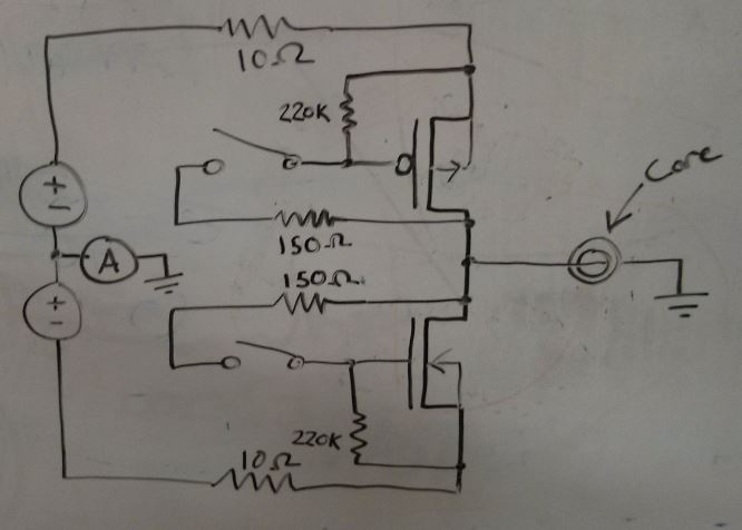
Crappy whiteboard drawing of my core test circuit.
Above is the circuit I ended up using. It employs a set of big TO-220 MOSFETs, one P-channel and one N-channel (I used SUP75P03 and IRFB4110, but you could use practically any other parts on hand). I used some more 150 ohm resistors (because they were already out on my bench) in series with a couple of small tactile switches as triggers, and put in some larger resistors from gate to source of each MOSFET to make sure they shut off when I open the switch. You could probably use any resistors within a decade of these values and it’d still work.
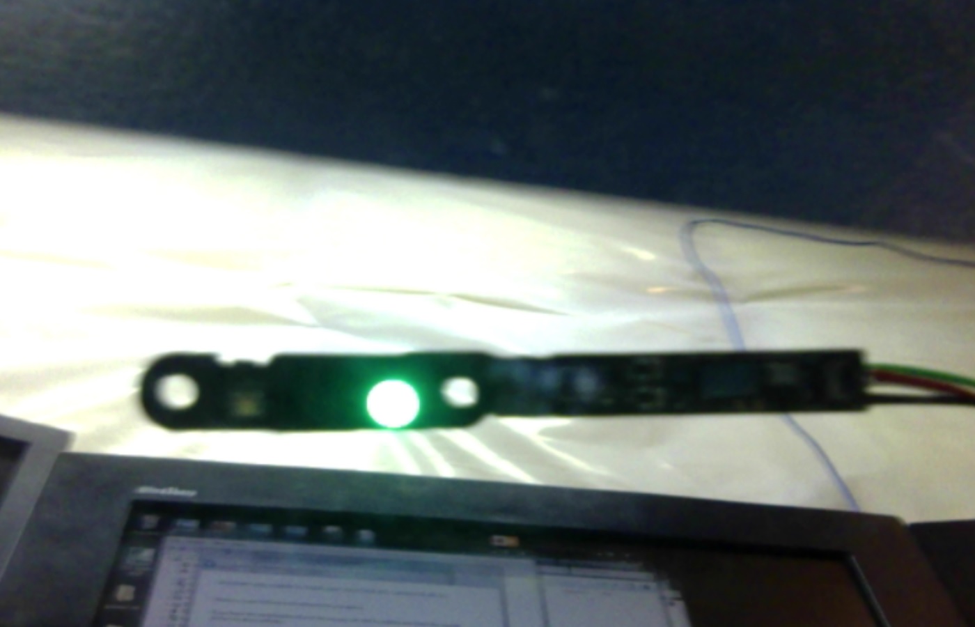
The circuit is driven by two bench supplies. In my case, this is in the form of one dual-supply which has voltage tracking, a handy feature which I originally used but which I eventually disabled for reasons I’ll get into later. There is a 10 ohm, 10 watt ceramic resistor in series with each supply. This is important, because you may be playing with quite significant currents, and it is all too easy to accidentally push both buttons at once and short out your supplies across the MOSFETs. This is also why i used TO-220 transistors – they will usually happily take hundreds of milliamps without any heatsinking. By the time I was done testing, both transistors and both resistors were fairly warm to the touch. Finally, there is an ammeter in series with the ground line, played by a handheld multimeter.
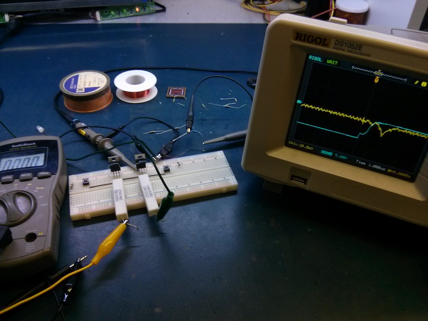
The test setup.
I initially set the bench supplies to about 10 or 12 volts and held one button, then adjusted the current limit to about 800mA, a little bit shy of the experimentally determined fusing current of the 36AWG core threading wire I used. I then held the other button and did the same. Alternating button presses, I set the scope to trigger at 20mV and a timebase of 1us/div. And, success! The scope showed clear pulses the first time either button was pressed, indicating a change to the magnetization of the core. Then subsequent presses of the same button produced no such pulses, and only a press of the opposite button produced a pulse as the magnetization was again flipped.
I then attempted to find the minimum required current for changing data on the core, but I got some troubling results. The core seemed to work down to a few tens of milliamps sometimes, and a couple of hundred milliamps at others. I soon found – and this is so important a point that it inspired me to write this post – that you cannot use a current-limited supply to do this test. Any capacitance at the output of the supply can cause a brief but large current spike which can unpredictably change the state of your core. Instead, use a voltage-limited supply and rely on the series resistors to limit the current through the transistors. You may also find that this simple circuit may not exhibit equal current output in “push” and “pull” operation. This is why I eventually stopped using the tracking feature of my power supply and ended up setting the two supplies manually at each step.
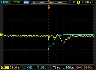
Scope capture of the signature of a changing magnetic field. With different component values and core material, your plot may vary.
Ultimately, through some trial and error, I found the required magnetizing current for my cores to be between 500 and 600 milliamps. This was a little bit disappointing, because I expected a much lower current that I could drive with small, cheap logic transistors. But I suppose it’s better to find out now than later. So now, on to the array driver design… but that’s a post for another day!