Welcome back! It’s been more than a month and a half since my last post on the Macbook Pro Retina panel – damn my “real job” and the time it consumes. But we’re here now, so let’s dive into things.
In the previous two posts on this subject, I have talked about two boards that I have been developing for the 15.4″ Macbook Pro Retina display assembly: a breakout for the FaceTime camera, and the main display controller / backlight driver board. Well, in the month-and-a-half that has elapsed, both boards have been received and built. Let’s start by taking a look at the former.
Camera Breakout
When I went to order these boards, I did so immediately after the cutoff for the current OSH Park 4 layer order, so the estimated delivery time was three or four weeks. Unhappy and impatient, I held off and instead ordered the board as 2-layer for more instant gratification. The two inner layers are only GND, so this is possible without too much trouble. It throws off the impedance of the USB traces probably significantly, but as the entire trace length is a half inch or so, I figured it’d be close enough for at least temporary use.
So the boards arrived a week and a half later. I immediately noticed something interesting and bothersome. Board fab houses typically require a gap between the edge of any copper and the routed board edge. If you are making a small board and including mounting pads for screws, the pads may consume a large percentage of the total board area – in fact, the pads may well drive the overall dimensions of the board, and larger dimensions mean greater board cost. I wanted this board to screw mount, but even the 2-56 screws I designed for needed quite significant pads. I decided it would be nice to trim the amount of room wasted on mount pads by clipping the pads at the board edge, allowing the screw to extend into the no-copper area at the edges of the board – it really only drops a few cents from the board in this case, but it makes me feel better.
So in Altium Designer, I made a small Pad on Multilayer (the magic layer which is copied to all other layers), then made a Polygon in the shape of a circle with a flat edge and also placed this on Multilayer. In theory, this should have resulted in a round pad with a flat edge, drilled and plated through as expected – in fact, the 3D render of the board shows this:
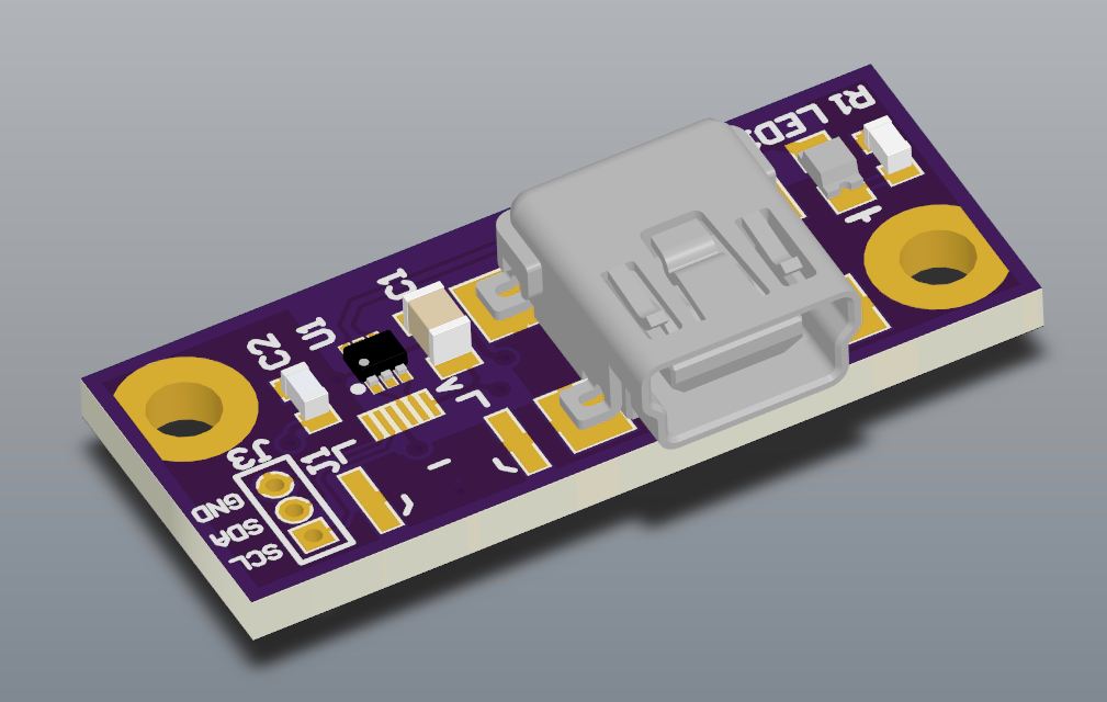
Mount pads look OK here.
But what arrived from the fab was this:
There aren’t supposed to be voids in those mount pads…
When I poured the rest of the GND polygon, apparently Altium attempted to connect to the inner Pad, and generated Polygon Cutouts surrounding it, which happened also to cut the Multilayer polygon. It didn’t show in the PCB editor, although it did in the Gerbers – but I was in too much of a hurry when ordering to notice. Oops. But so be it, it’s only the mount pads.
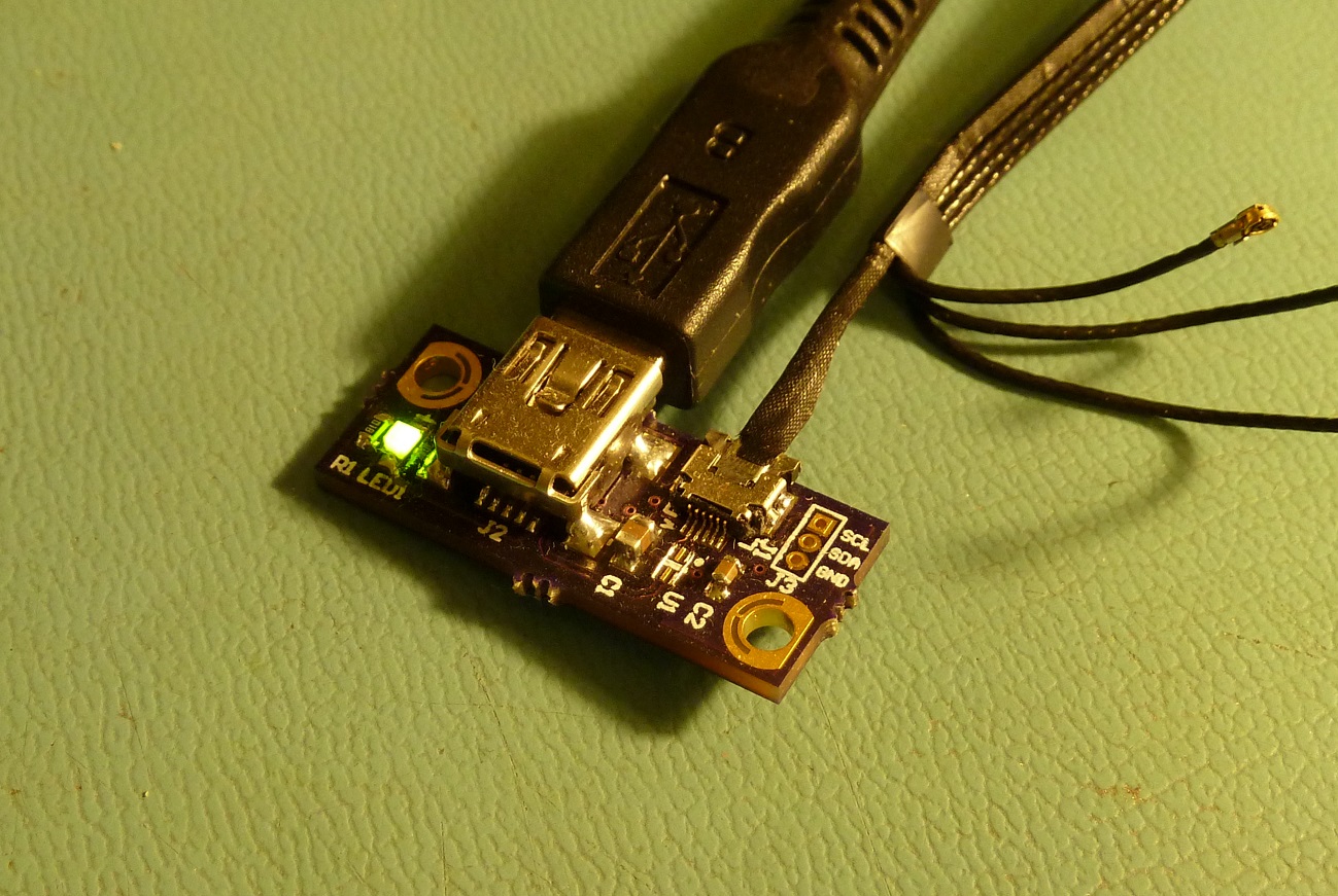
I then assembled the board, and with bated breath, plugged it into a USB port. And Hooray! The Device Connected sound sounded, and the camera showed up in device manager. But, strangely, the power LED was orange. I specified a green LED, I thought I placed a green LED, but it was bright orange. I checked the package to be sure but it was correct. It was then that I discovered a tiny short, and simultaneously learned that if you apply 5V directly across a 2.1V green LED, it becomes an orange LED. Neato! It also gets real real hot. But miraculously, after I corrected the short, which had caused the full USB voltage to appear across the LED, it returned to green and operated as normal. So I guess I can say, these OSRAM CHIPLED parts seem to be pretty hardy! I unfortunately don’t have any photos, but these parts are cheap, so buy some and experiment for yourself. Science!
After a few days the 4 layer board order deadline had arrived again, so (having not discovered nor corrected the pad issue) I re-ordered the board as 4-layer, this time adding a second transient suppressor for the ALS connector… because why not, and you can always short it with jumper wires if you don’t want to use it. So here’s what that looks like (note that I have fixed the pad issue at this point):
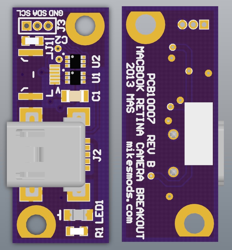
Yep.
I haven’t bothered to build this one yet, but it hasn’t changed significantly since the 2-layer version, so I suspect it’ll work fine. The files for this board can be downloaded here:
- PCB10007 REV B GERBERS (13K ZIP)
- PCB10007 REV B LAYERS (22K PDF)
- PCB10007 REV B STENCIL (1K ZIP)
- SCH10007 REV B (49K PDF)
Enjoy!
Main Controller Board
Now, the information you’ve all been waiting for. As I said on the previous post on this subject, I quickly threw together this board to get it in before the following OSH Park cutoff. As such it’s not perfect, but it is fairly functional (or so it seems from the minimal amount of testing I’ve done so far).
There’s a lot of new stuff going on on this board, as compared to my iPad board (on which this one is loosely based). Of course the panel output connector is different, because the panel is different. Also, though, the barrel jack has been removed, and a 2-pin shrouded connector has been added in its place. Barrel jacks, I finally came to realize, are just too damn big and expensive for a little cheap board like this. The new solution is less than a dollar in single quantities for plug, receptacle and terminals, whereas the board mount barrel receptacle was more than a dollar by itself, not counting wire mount plug. Plus the barrel jack tended to be the tallest component on the board, driving enclosure dimensions. It takes a bit more work to implement, but I still think this was a good change.
The dc-dc converters are new as well. The board contains two dc-dc buck regulators, both based on the AOZ1281 from Alpha & Omega Semiconductor. This part was chosen due to very low cost – about $0.90 in single quantities – as well as ample output current (1.8A) and acceptable input voltage range (3-26V). The board implements this part as one 3.3V/500mA converter and one 3.8V/1A converter, the former for processor, indicators and other functions, and the latter for the panel itself, which was investigated and found to run well on 3.8V in a prior post. It’s probably a 5V panel, in retrospect, and I may someday become ambitious enough to test it at this higher voltage, but for now 3.8V works.
The board shares the same Freescale MKL25Z128VFM4 processor as the iPad board, again due to cost to performance ratio of the $3 ARM Cortex-M0+ core. Sure, I could drop $0.50 and put in a MSP430, but I like the potential for other functions that the more powerful processor enables. I still need to learn how to program the damn things, but I digress. The other big IC on the board, the backlight driver, has completely changed compared to the iPad version. Whereas the iPad panel has 12 backlight channels at 20V apiece, the Macbook has only six channels but at some 52V. The LT3754 used on the iPad board only does 45V, so a new backlight driver is needed. Of the (relatively few) integrated boost converter / LED driver ICs, the best choice for this application seemed to be the Freescale MC34844A, which happily will push out 60V with appropriate configuration.
In the interest of keeping this post from being more than fifteen or twenty pages, I’ll leave the rest of the description to the schematic, but if anything is unclear please feel free to drop me a comment or email.
Again, this board uses 2-56 mounting screws, and again, I opted to include clipped pads. And again the boards showed up with voids in the pads. But this time, inexplicably, some of the pads did not have voids. They were all created the same way so I can’t quite explain that one yet. But one thing is for sure, I’ll certainly pay more attention from here on out. I built the pads for one of my boards at work with clipped edges as well, but this time used top and bottom polygons instead of one multilayer one. In this way the pads are slightly smaller in the internal layers, but on the other hand the polygons connect without issue, so that’s a small price to pay.
Anyway. Here’s the (99%) finished board, lacking only a fuse and transient suppression diodes in front of the USB port and DP connector:
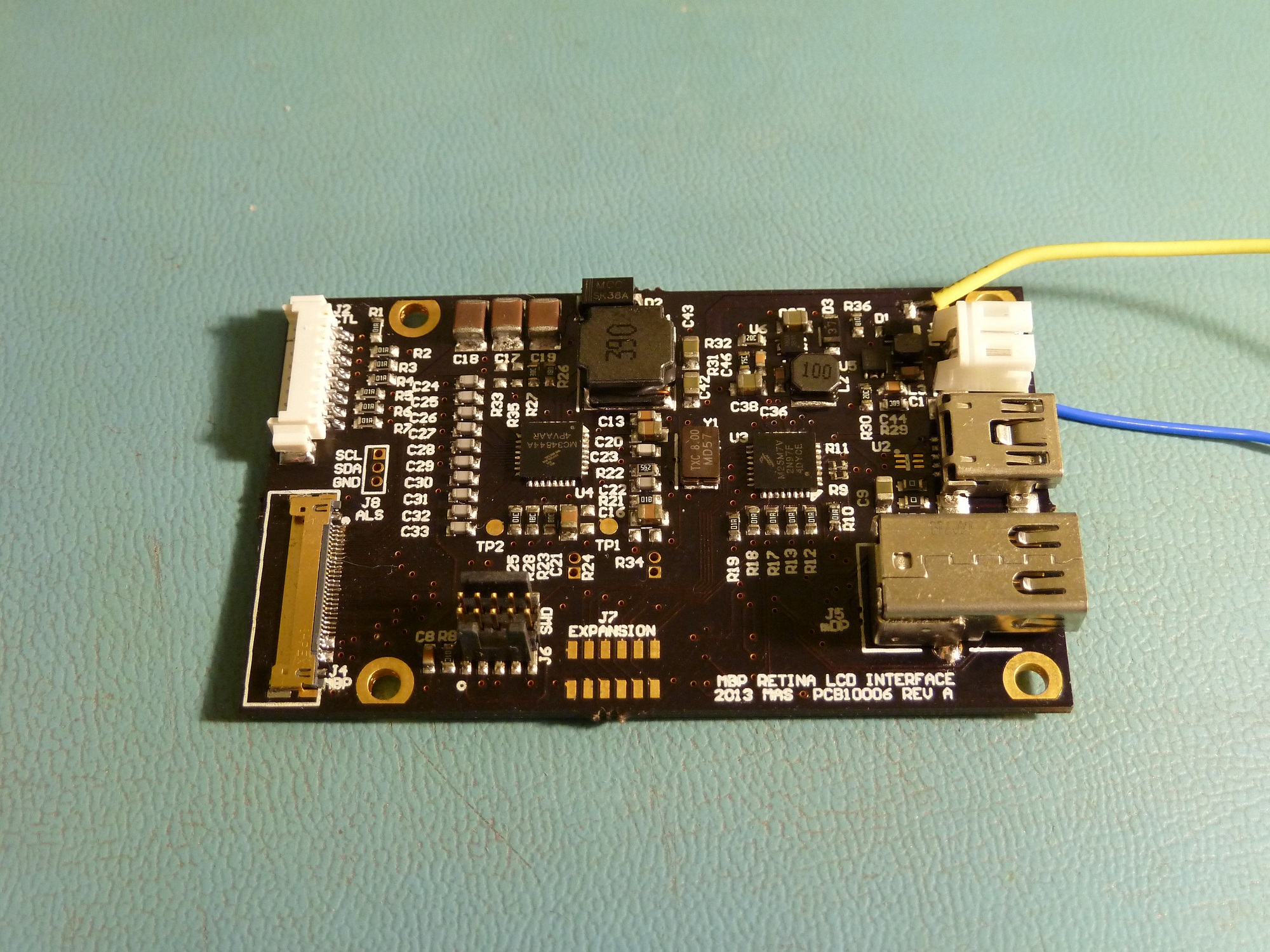
Top. Ignore the soldered-on power wires.
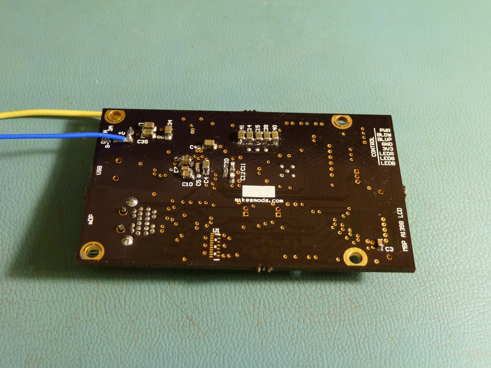
Bottom.
I’m not 100% happy with it – in particular, I suspect that my overzealous attempt to match the lengths of the DisplayPort lanes may have actually had an adverse effect on signal integrity as the traces have to bend a whole lot and come in much closer range of each other than is really recommended. But I can say that the board works like this, and I can’t keep from releasing something forever because I’m not 100% happy with it (or so my boss always says – “You can always fix it in Rev B”). So here we are.
Now, the processor has control over panel power and backlight on/off and brightness, so without programming the processor the board won’t do anything. So, still lacking much experience with the ARM Cortex-M0+ platform, I wrote a very barebones program that simply turns on the power and backlight driver for the panel, and additionally powers up the PWM controllers for the offboard indicator LED. So here’s the board documents, and the source to at least power-on the necessary systems:
- PCB10006 REV B GERBERS (76K ZIP)
- PCB10006 REV B LAYERS (107K PDF)
- PCB10006 REV B STENCIL (3K ZIP)
- SCH10006 REV B (103K PDF)
- TestPCB10006 (CodeWarrior project, 62K ZIP)
Holy cow, I just realized I never released the documents for the indicator/button board either! Well, let’s go ahead and do that now too. Here’s what it looks like:
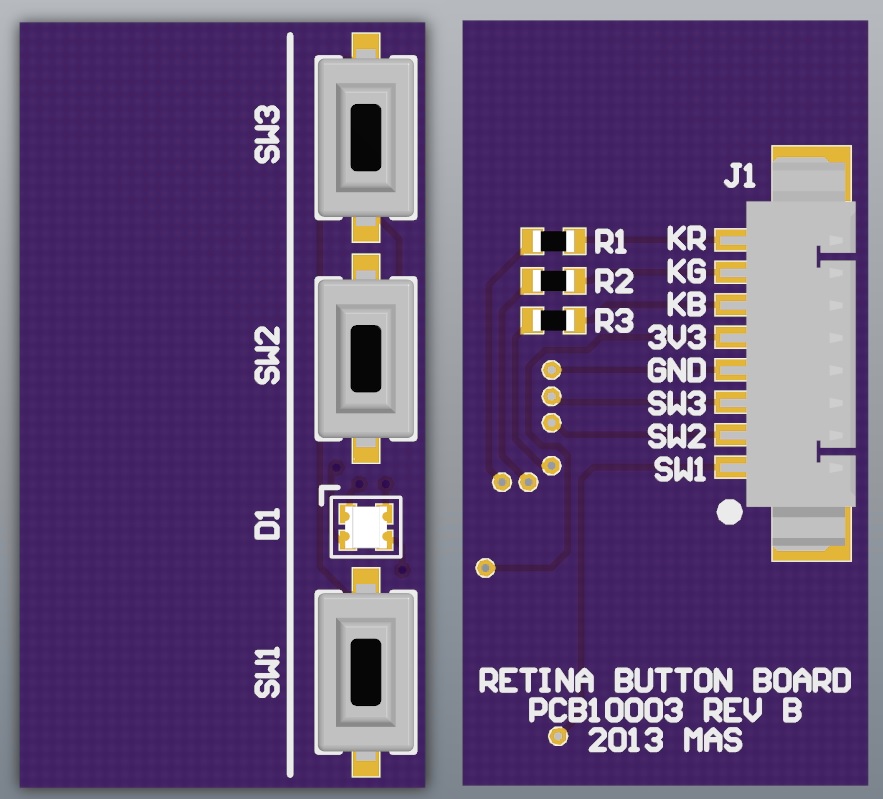
Pretty simple.
This board is designed to be double-stick taped directly to the back of a panel at an edge of your choosing (my preference is bottom-right) and connected to the main board via a wire harness. Some of the other controller boards out there with buttons onboard have very awkward button placement, so this is a slightly more expensive but much more elegant solution. The files for this board are attached here:
Whew. This has been a grueling post to prepare. Enough for now. Er, except for one last picture!
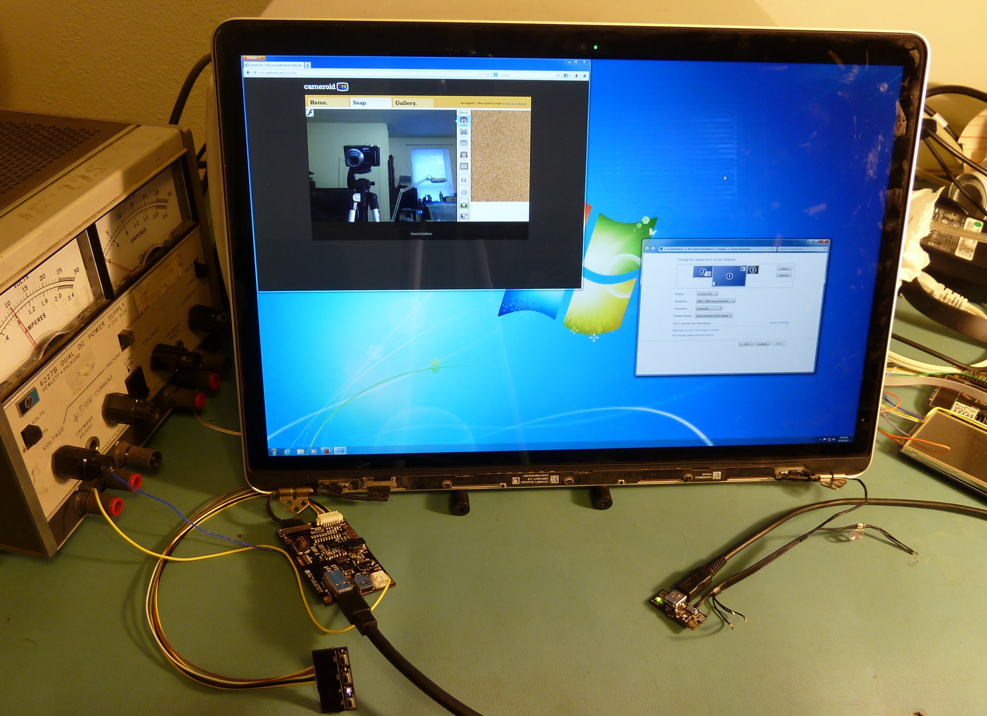
Woohoo!