Something new and interesting.
So, my breakouts for the Macbook Pro Retina’s I-PEX display connector are finished and are on the way from the supplier. This has been a long ten days. But it’s not all roses, they’re set to arrive on Monday, the day I start a week of travel for work. So there will be no fun display hacking time for the next week. Oh well.
But in the meantime I have turned my attention to the other bundle of cables coming from the display – the antenna and camera connections. The antennas aren’t all that interesting – we could use them, but they don’t provide a function on their own and the hardware necessary to make use of them would be more complex than it would be worth. Plus both of my displays have the antenna wires cut. On the other hand, the camera is a bit more useful. And like the panel itself, it can be made operable with little more than a connector breakout.
Apple cameras (“iSight”, or more recently “FaceTime”, embedded cameras) have been USB based for a number of generations of MacBook, since at least 2006. Similar to normal USB, the camera connector traditionally contains 5V, GND, and two USB data lines. However in addition to this, most Apple camera connectors also carry an i2c interface. We’ll talk about that a bit more later.
There are plenty of different Apple camera units, a unique one for each model and generation of Macbook. Over the years they have been built in a number of different form factors, and have been terminated with several different types of connectors. And within these connectors, the wiring has been arranged in several pinouts. So while I have some Macbook schematics and know what to expect in general, it is not so easy as applying a “generic” pinout to this unit.
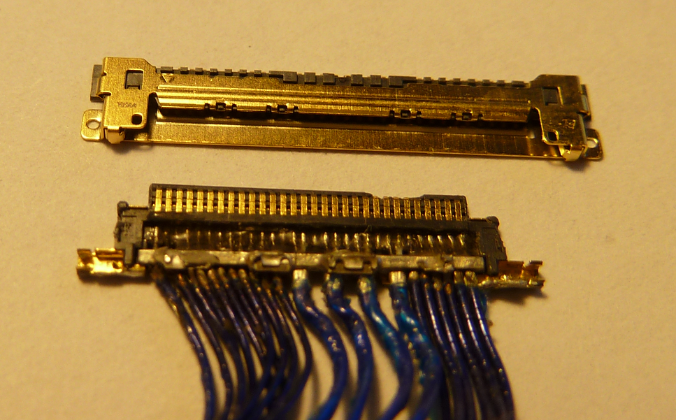
The Macbook Pro Retina display assembly’s camera connector is made by ACON (Advanced Connectek); the part number is currently unknown. It’s a six-position connector with 0.4mm pitch, likely a solder-type part as the flat contacts appear to be integral to its body. A bead of epoxy seals the wires into the connector. Six individual black wires run from the connector to the camera. The wires are somewhere in the 0.3-0.35mm diameter range, stranded, and uniquely jacketed – the black jacket appears to have a copper coating on the inside. The wires are bound together with sticky black fabric tape and enter the display assembly on the righthand side of the bottom edge after about 150mm of free cable tail. On the way it passes through the righthand hinge assembly.
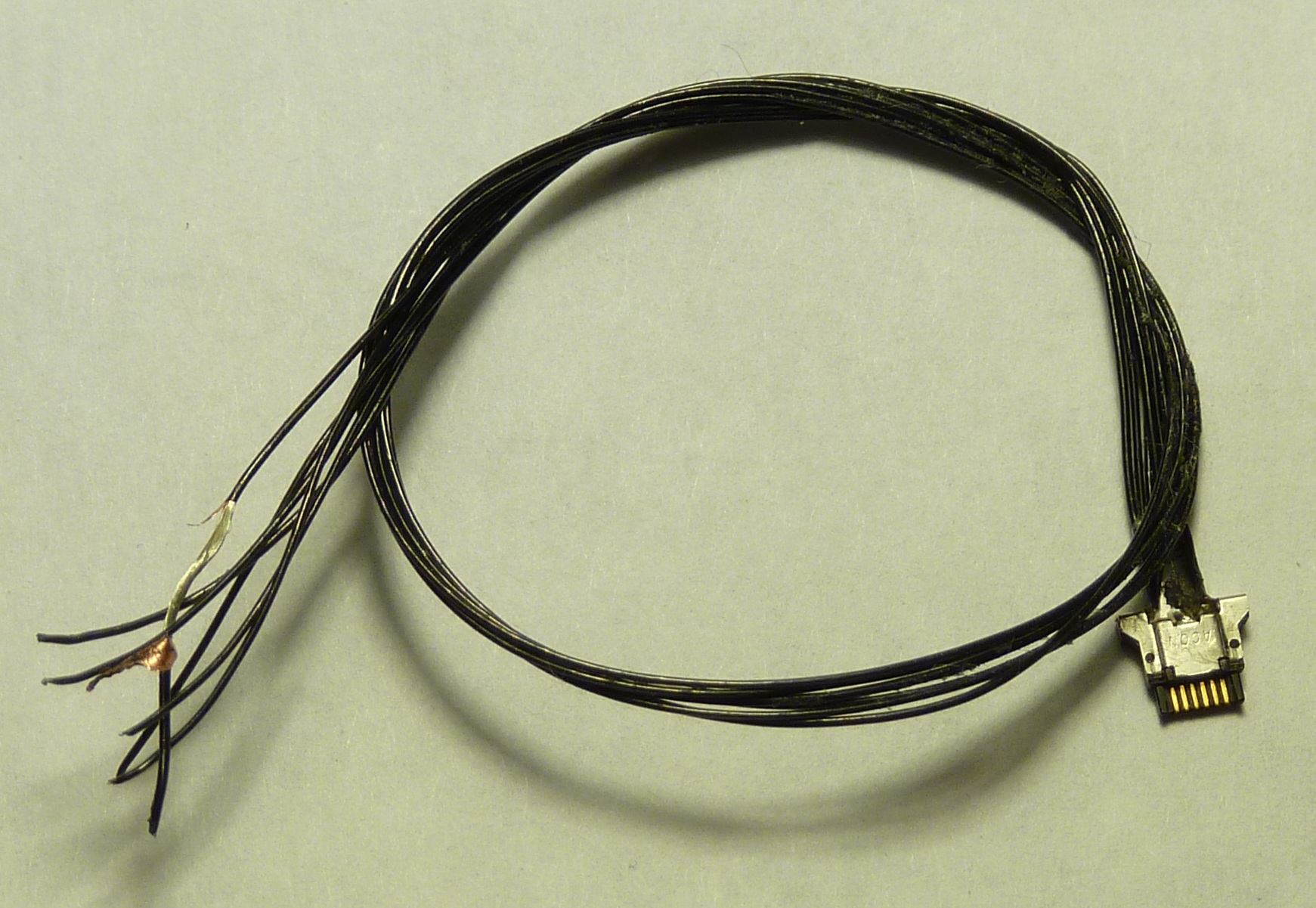
A Macbook Pro Retina camera cable, cut off a panel. The copper foil jacket can almost be seen in the stripped wire to the left.
The camera module sits behind the main display glass. According to the iFixit teardown of the Retina display unit, the glass can’t be reliably removed without damaging it. Therefore it would be best to figure out the pinout without having to inspect the camera board directly. The ideal way to do this would be to pull the pinout directly from the schematic, but as I have not yet found a schematic for the A1398 Macbook Pro, we must devise another way.
One way or another, a mate connector for the camera would be desirable, to avoid having to cut the cable. As I have been unable to find a source of these directly, I bought a Macbook Air camera mainboard sans lens. I was very careful to inspect the myriad Macbook cameras available, because many of these – INCLUDING the A1398 camera – appear to use FFCs or other types of connectors, which will not mate with the motherboard side of the camera harness. Here’s the board I bought:
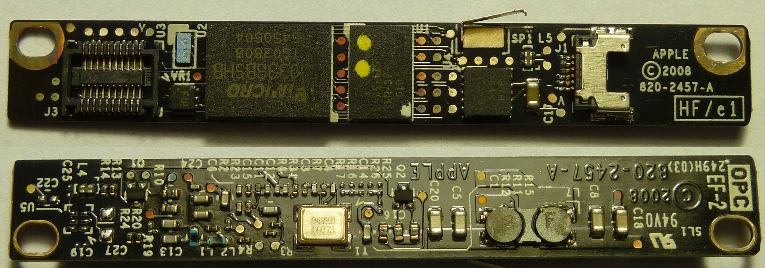
Macbook Air camera mainboard, unknown source model
The side advantage of having an additional camera board to fondle is the ability to probe and investigate how Apple designs their camera boards in general. So what have we here? First we will evaluate the silicon present on the board. The most prevalent IC is U2, a Vimicro VC0336BSHB USB webcam interface ASIC. From the product brief, we can see that this chip talks to a CMOS image sensor over LVDS, has a serial interface for a flash memory, has mic inputs and an AC’97 codec interface and speaks to the PC over USB.
Next to this is a SST SST39LF010 1Mbit flash memory, which is probably where configuration information such as the USB device descriptors are stored. Next to this is a suspiciously placed chip with a pair of inductors underneath, which predictably is a dual buck regulator, a TI TPS62402DRC (marking BYH). This IC provides a fixed (1.8 or 1.2V)/400mA and 3.3V/600mA.
That’s enough to work with. The datasheet for the TPS62402 notes that pin 8 is GND and pin 3 is VIN. Some probing reveals that in the input connector beginning at the left (marked with a silkscreen arrow), pin 1 is +5V and pin 6 is GND. This is reaffirmed by the connection between GND and the metal body of the connector. While we’re at it, EN1, EN2 and DEF_1 are pulled to +5V, meaning both supplies are permanently enabled, and the output voltages are 3.3V and 1.8V.
Conspicuously, two of the remaining pins (4 and 5) are run through a common mode ferrite bead. This wouldn’t make sense for an i2c SCL/SDA line, since the two signals are not complements of one another and would be attenuated by the bead. So we will guess that these are the USB connections, and the remaining two (2 and 3) must then be i2c. Probing the i2c lines to random points on the board indicated that the lines run through the J3 board-to-board connector that connects the image sensor daughterboard. We’ll remember that for later.
That was enough of this board. Now, on to the real deal. We know that the shield of the connector should be connected to GND. If we are very lucky this will also be true on the opposite end of the cable – fortunately we are, and it is simple to confirm that pin 6 (as mated to the Air camera board) is GND as it is tied to the metal body of the connector.
Now for the 5V line. Most power rails have some sort of capacitance to ground to smooth the line when brief current pulses are drawn from it. In the Air board, measuring across the known power leads returns an input capacitance of 8.8uF. Measuring any of the other leads to ground returns much smaller capacitances. So this seems to be a reliable way to locate +5V.
We can guess that +5V should be pin 1. But no! Measuring the capacitance between this pin and the metal connector shell on the panel revealed a fairly insignificant capacitance. In fact, when the rest of the pins are probed, only pin 3 exhibits a high (6.3uF) capacitance indicative of the +5V pin. So immediately, the pinouts are different.
Knowing where the voltage rails are located is enough to work with. If I was desperate I could use the same method for finding the rest of the pinout as I plan to use on the display connector – connect one pair at random, see if it enumerates, if not, reverse it, if it still doesn’t, swap for the other pair and repeat. But I decided to cheat a bit and researched the Macbook schematics that I have to see if Apple had previously used a pinout with Ground, two skipped pins, then 5V. I found the answer to this in the schematic for the Macbook Air A1370 LIO board – a pinout with GND as pin 1, 5V as pin 4, and two USB and two i2c pins:
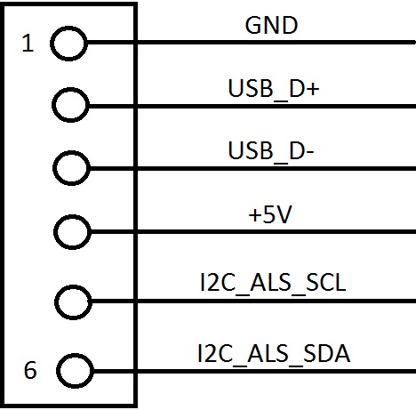
A MSPaint rendering of the Macbook Air camera connector pinout at the LIO board. The actual schematic is available on the internet, go look for it if you’re curious.
This is very valuable information. First of all, it notes that the pin numbering on this side of the board is different than the silkscreen on the Air board, placing GND as pin 1 instead of pin 6, etc. Second, it makes the pinout (1-6) GND, USB_D+, USB_D-,+5V, I2C_SCL, I2C_SDA – this makes a lot of sense, as the pinout for normal USB connectors is +5/D-/D+/GND.
So without further ado, let’s see if this pinout is accurate. I pulled the socket off of the Air board with my hot air station and wired it to a cut USB cable.
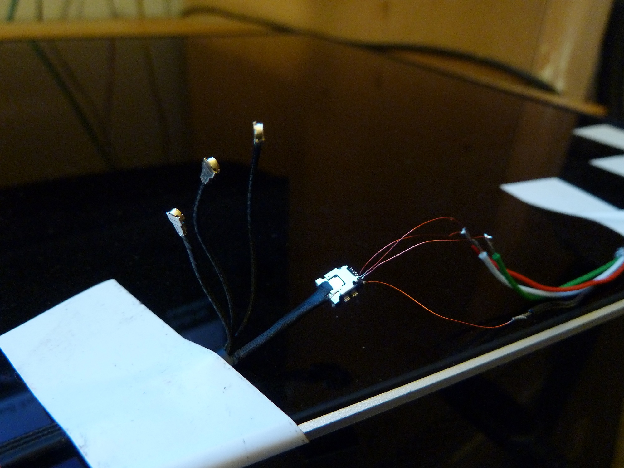
This wasn’t much fun to solder.
Now, when connected to the USB port, gasp! New devices!
Holy cow, it’s alive!
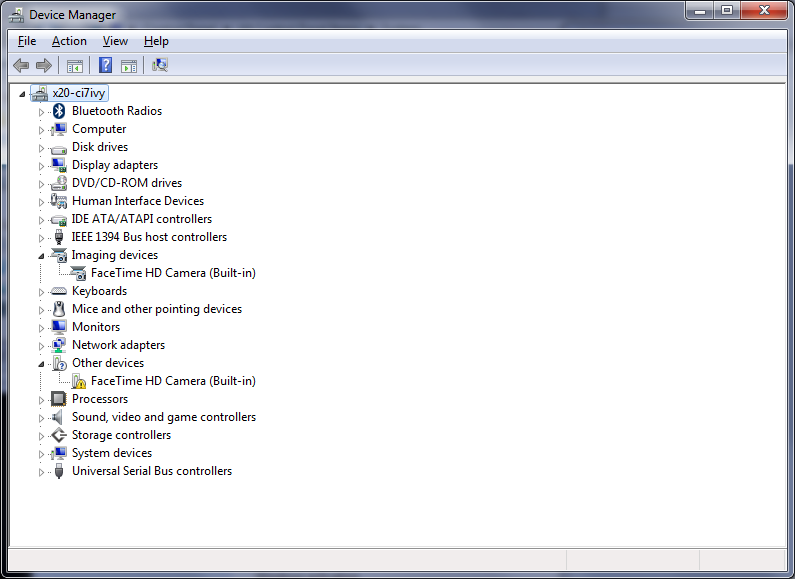
The camera enumerates as a USB Composite Device (USB\VID_05AC&PID_8510&REV_8025) with two sub-devices, both identified as “FaceTime HD Camera (Built-in)” (USB\VID_05AC&PID_8510&REV_8025&MI_00 and _02). The _00 device installs automatically with generic Windows imaging device drivers; the _02 device claims no drivers could be found. The solution is probably to dig through the BootCamp drivers and find one, but that’s a headache for another day.

The camera enumerates as these three devices. Not sure why it finds drivers for one but not the other. Nor, for that matter, why it’s two cameras…

But despite the questions, hooray! It works!
So there you have it! Camera operational, simple as that. But what about the i2c connection? What does it do? The answer to that is in the schematic as well. The netnames are “I2C_ALS_SCL” and “I2C_ALS_SDA”. These are the communication bus for the Macbook Pro’s ambient light sensor. I will leave the protocol hacking of the ALS for another post.
For those who wish to hack around with the camera and ALS, I have drawn up a simple breakout board with a camera connector, a mini-USB, and a 0.050″ header for the ALS. I’ll post files for that board here as soon as I get a chance. Remember though that I don’t have a source for the camera connector mate socket, so you’ll probably need to source a used camera board with the appropriate connector and harvest it. The price is not bad; I paid about $6 for mine.
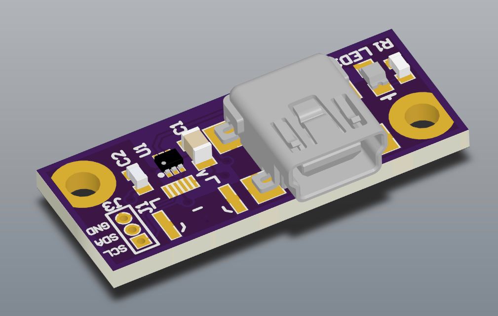
For a sense of scale, remember that that’s a miniUSB…
That’s enough for this installment. Next time, hopefully I’ll be showing off the working panel.
<< Previous post in this series … Next post in this series >>