As I alluded to in previous comments and update posts, I have received and built up the boards for the simple breakout. I used a sharpened toothpick to apply solder paste to the board, and reflowed the board in my toaster oven. I have noted a couple of issues with the first revision of the boards:
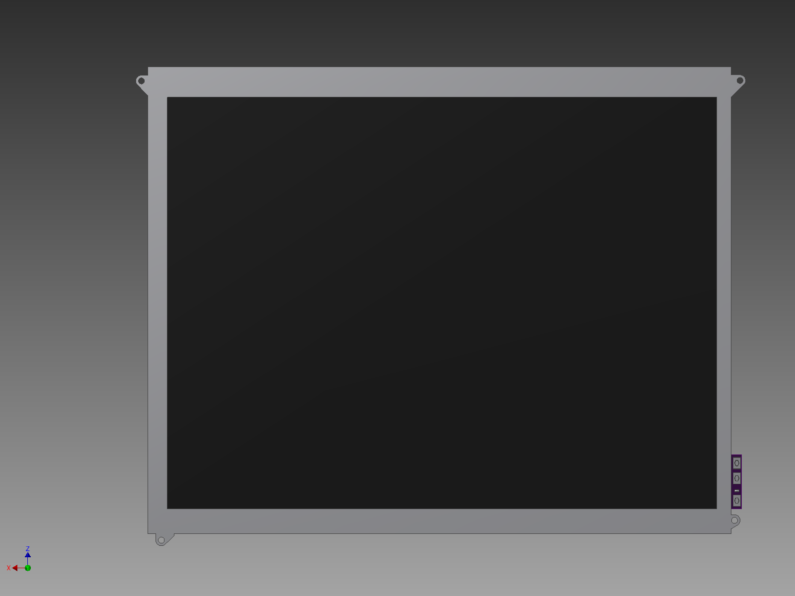
- The backlight power pads are through-hole. Care must be taken to keep the backlight leads flush with the board or they interfere with the panel FFC.
- The connector for the panel has contacts on both top and bottom. This makes it possible to electrically connect the panel backwards. The DisplayPort connector is on the other side of the board, which makes it reasonable to expect the panel to be plugged in backward.
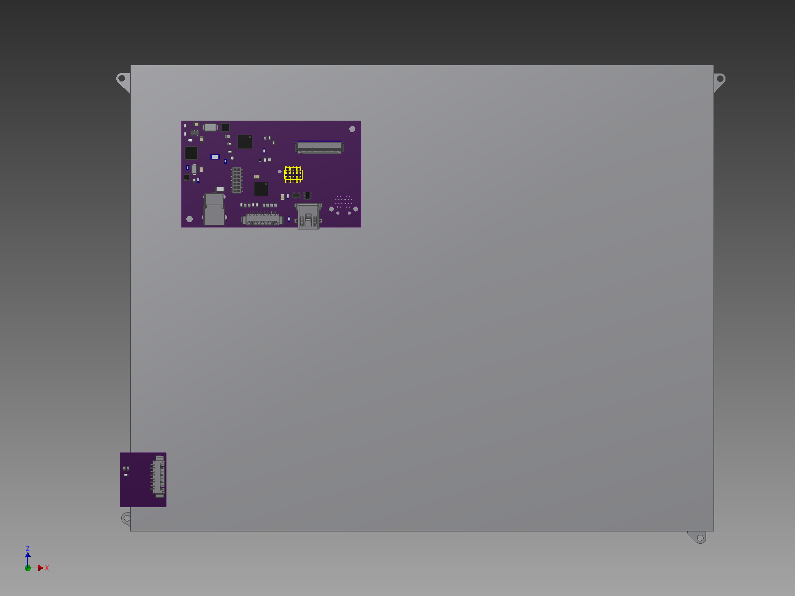
- With the DP connector on the back, it makes the board awkwardly arranged – it can’t be affixed flat to the back of the panel. It was designed to be free-hanging on the cable since it is meant as an interface for those using the panel in a projector, but it would be nice to have an alternate mounting method for those who want to use the panel as is.
- FInally, and most seriously, I accidentally used the source-side pinout for the DisplayPort connector. In the source connector, from pin 1 the lanes are numbered 0, 1, 2, 3; in the sink connector they are mirrored. This results in Link Failure errors on the host system. This was an important lesson, and one which I’m actually glad to have discovered after only $50 worth of boards, instead of at work where I am also working with a DisplayPort design but where the cost would be closer to $3000.
The first three issues were workable, but the last one meant the board was inoperable. But with an Xacto knife and some 36AWG magnet wire, I was able to make the required changes. The finished board looks like this:
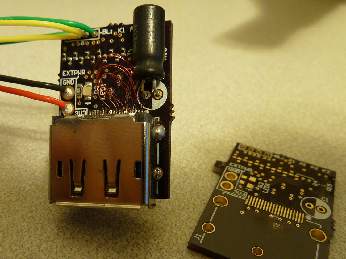
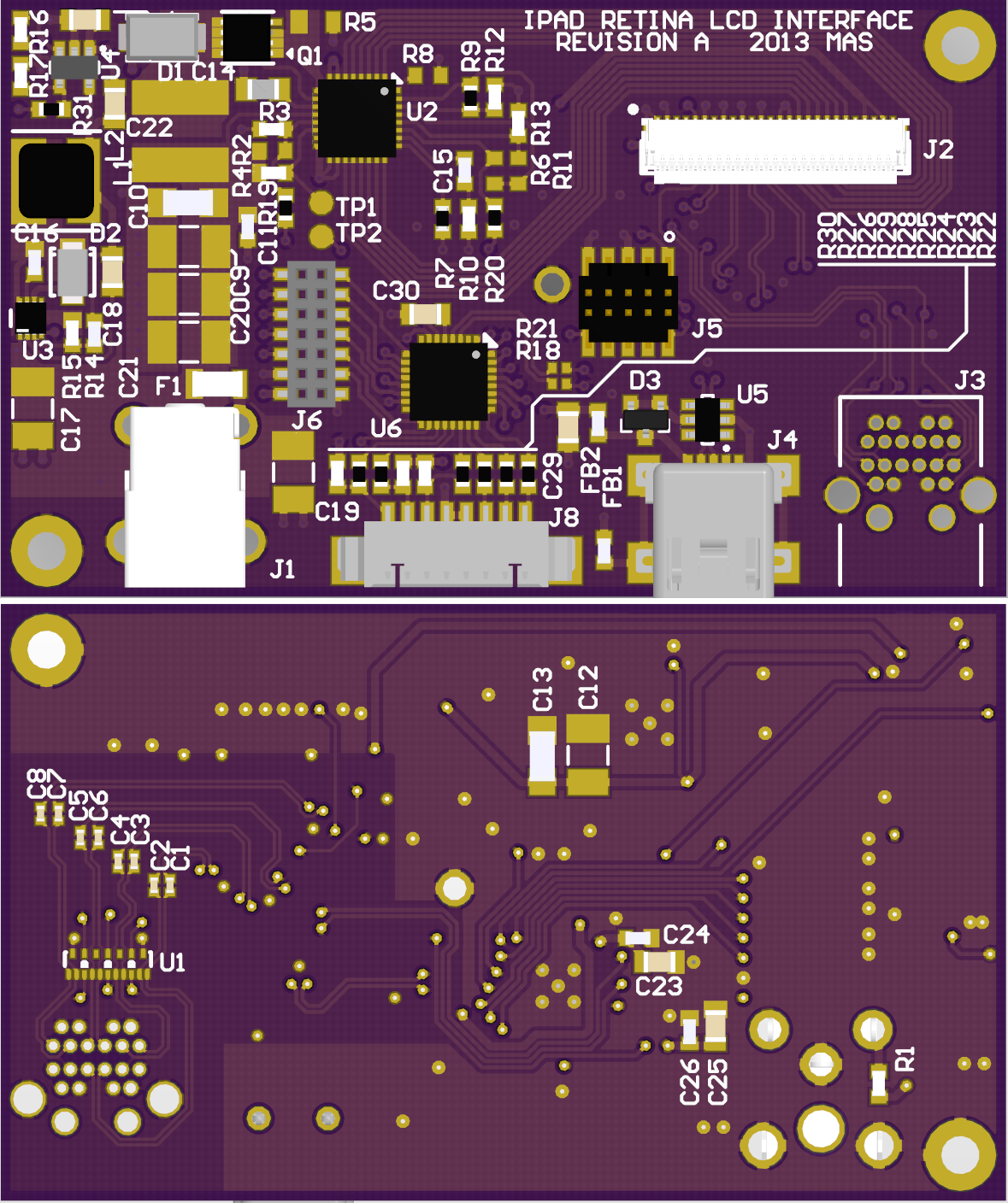
Front view. Note the magnet wire modifications in the center.
Rear of board. Ignore the flux mess.
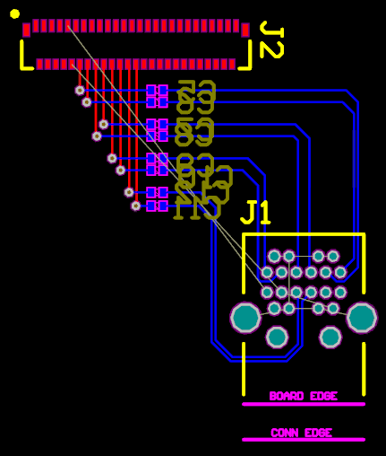
If you happened to order the Rev A boards, you too can make the changes. You will need to cut the DP traces at the rear of the connector, and again at each of the vias where they are transported to the bottom side. You could conceivably leave one or the other of them connected, but it is improper to leave such a long stub on a high-speed data line as it distorts the signal and causes reflections. Then connect the vias back to the connector in reverse order. The modifications are as follows:
Cut at the red marks, install wires across the green and blue lines.
I would suggest soldering the wires to the back of the DP first, then threading the wires through the vias and soldering them in place. I think this will produce a more robust and neater end product. I soldered the wires in the vias first, and finishing the other end was a tremendous pain.
After making these changes, the board works great! I am very pleased with the project so far. The panel looks great – plenty of brightness, and super high resolution. Regarding brightness, I installed 100-ohm resistors and ran the panel at about 19.5V.
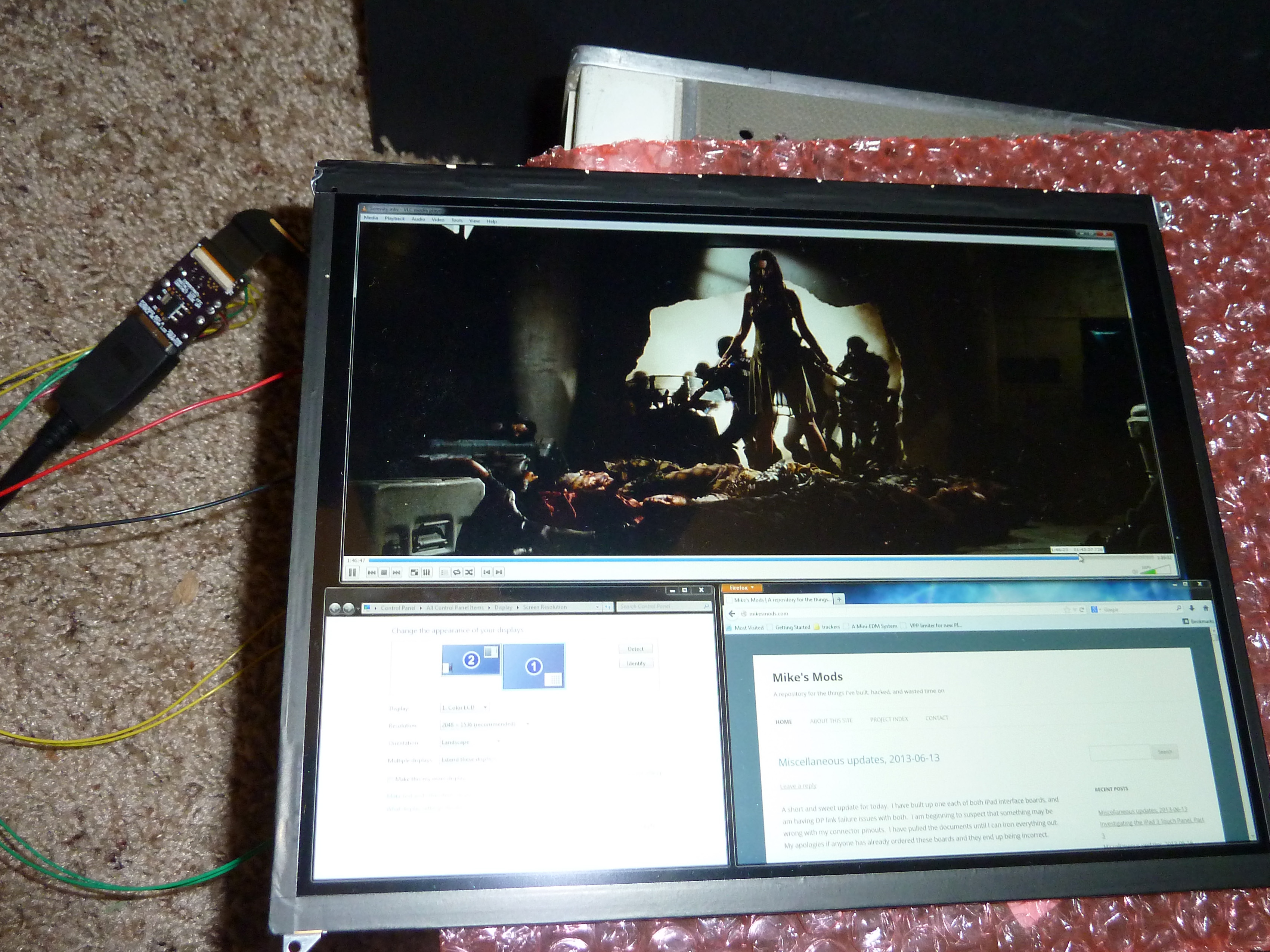
First panel test. At top is a 1080P HD movie at full scale. Plenty of screen real-estate!
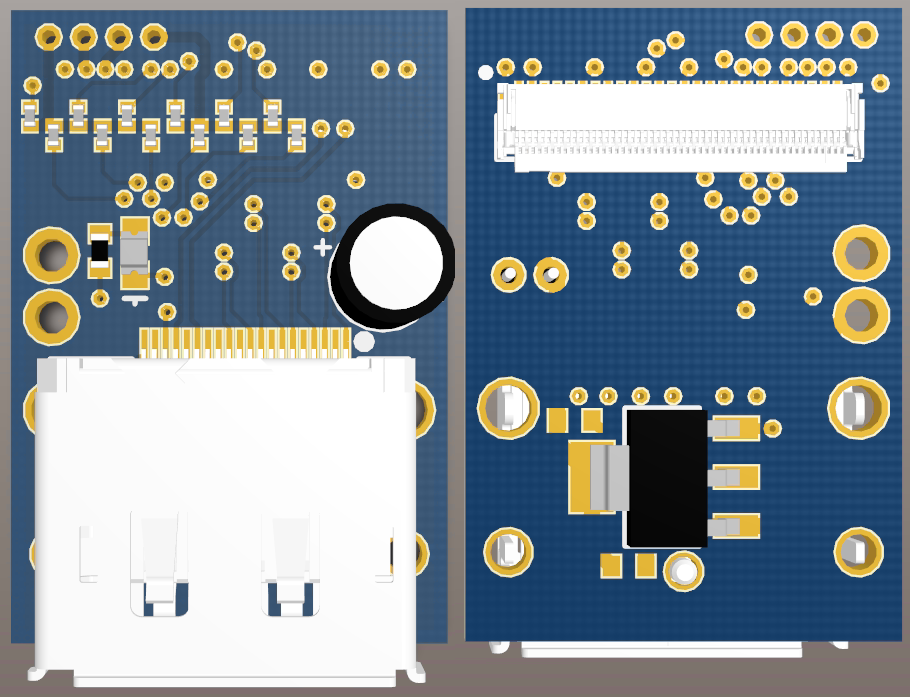
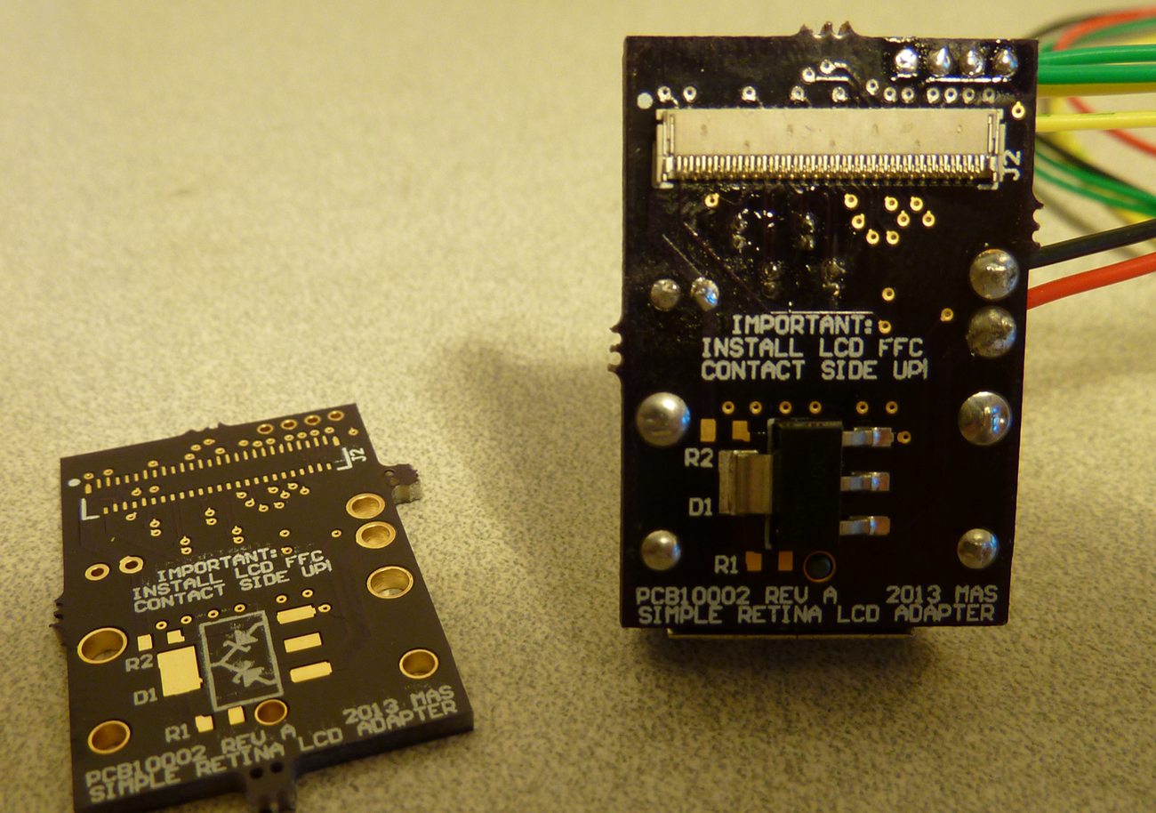
I have made the necessary changes to the board. As it works out, when the pinout is corrected it makes more sense to have the FFC and the DP connector on the same side of the board. This has the side effect of making the connection orientation more obvious, and allowing the board to be rear-mounted to the panel. I have also increased the size of the backlight pads, so the wires can be more easily surface-soldered and not stick through and interfere with the FFC.
I also had the opportunity to correct the trace size for the proper dielectric constant of the laminate. The OSH Park stackup is as follows:
- 1 oz copper (1.4 mil)
- 6.7 mil prepreg
- 0.5 oz copper (0.7 mil)
- 47 mil core
- 0.5 oz copper (0.7 mil)
- 6.7 mil prepreg
- 1 oz copper (1.4 mil)
For 1 oz copper with a 6.7 mil height over plane, using dielectric constant of 3.66 for FR408, and assuming minimum 6-mil spacing, to maintain 100 ohm differential impedance, Saturn PCB Toolkit calculates necessary trace width of 8.1 mils. I used the Saturn built-in value for FR408 when I originally designed the board, which is a little different and called for slightly smaller traces. Using the new trace sizing and the new board layout, I was easily able to make the traces all very near to equal length (506 +/- 2 mils). This is closer than they usually come out without a large amount of effort – in this case the board modifications only took an hour or two.

Simple interface adapter, Rev B.
The new boards are on order and should be in house in two weeks or so. I’m pretty confident now that I’ve tested the hand-wired version, but I was also confident when I originally released this board so it’s at your own risk if you want to order these boards yourself. Here are the board documents (now with pad masters, in case you want to order stencils):
- PCB10002 REV B GERBERS (22K ZIP)
- PCB10002 REV B LAYERS (253K PDF)
- PCB10002 REV B STENCILS (1.1K ZIP)
- SCH10002 REV B (201K PDF)
<< Previous post in this series … Next post in this series >>