I mentioned in the initial post of the iPad 3 LCD project log that I purchased an iPad 3 digitizer in addition to the LCD. I don’t want to call this article “Hacking” the iPad 3 Touch Panel, because I’m not sure how far I’ll get with it. But I want to at least make a page for this in case my findings may be useful for anyone attempting a similar project.
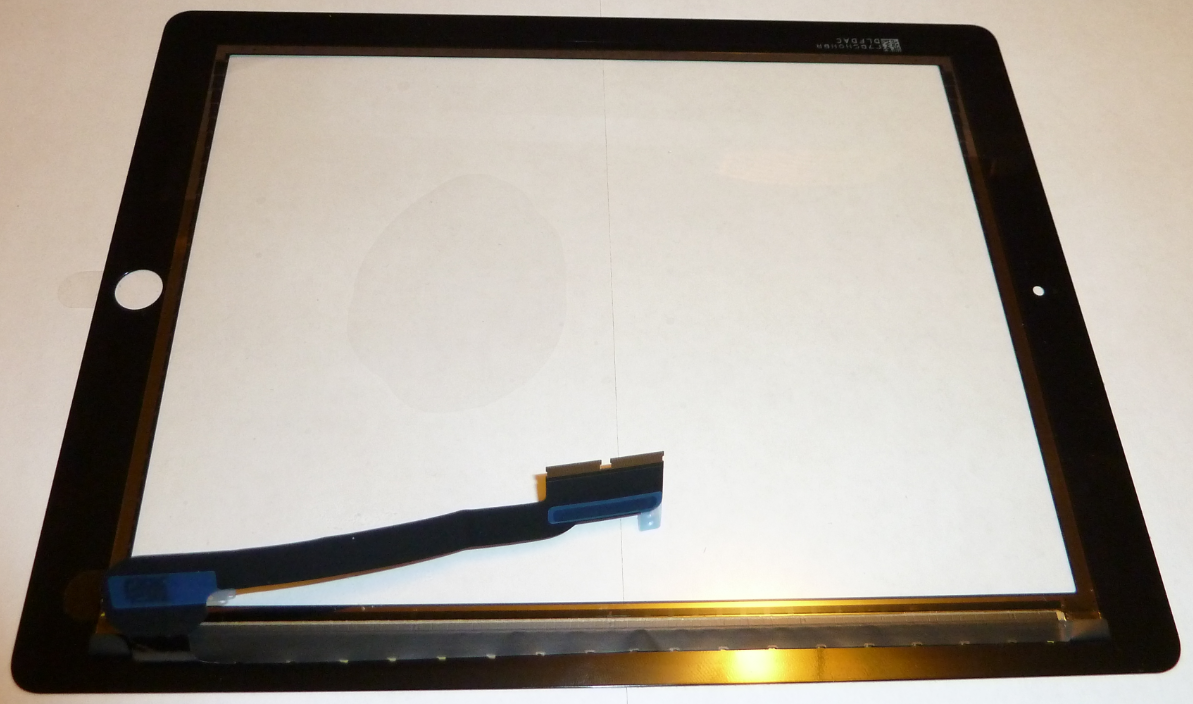
The full digitizer, as seen from the back.
This is a digitizer for the 9.7″ iPad 3 display panel. It is, per Apple’s website, “capacitive multitouch”, although the particular type of capacitive is undocumented. It is likely to be projected capacitive or some derivative thereof. The connector at the center is a 2×37 pin, 0.3mm pitch FFC. The contacts are on only one side of the flex cable, so a connector such as Molex 503566-3700 should be compatible.
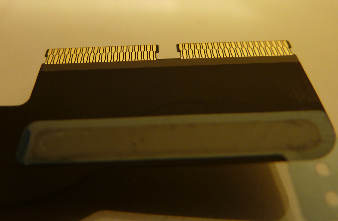
2×37 pin, 0.3mm FFC. Quite small.
The cable does not appear to have any embedded electronics. It is connected to the digitizer for about three tenths of an inch at bottom left and right in the above photo (top left and bottom left in the assembled iPad), and is glued down and appears to be occasionally connected along the remainder of the length. Looking closely at the connection points, we can see how the contacts are structured:
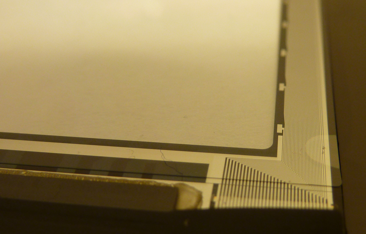
One contact interface. This would be at the upper left corner of the assembled iPad. Comes complete with dust under protective plastic film, and has been customized with black fibers.
The contact structure of the transparent section of the panel is typical of a mutual type projected capacitance design. Forty-one very fine wiggly lines travel unbroken from left to right across the iPad display, while thirty rectangular contacts along top and bottom (as seen above) frame four short wiggly horizontal line segments between each unbroken horizontal line. All horizontal lines terminate at a single contact on the right side of the iPad display and are individually connected at the left; all columns of line segments are bounded at both top and bottom by rectangular contacts (but are not in physical contact with them). I have tried to photograph the pattern with a microscope, but it is very difficult, so I have illustrated the basic idea below.

Pattern of sense lines on the iPad digitizer. Note that the digitizer is shown here on its side. Ignore the poor MSPaint rendering.
The effective resolution of this touch panel is then 41×30, but of course by interpolating between points a position can be calculated to much greater accuracy. It also explains the number of pins on the connectors – with 74 available contacts and 41 row + 1 row common + 30 column, only 2 pins are yet to be identified – although much work remains to map the functions to the pins.
Things are already looking quite good for getting this panel to do something. With a waveform generating MCU and a little math, this may well be workable.
That’s enough on that topic for today. See you next time.
I’m not sure if you’ve found the iPad 3 schematics, but the pinout of those two connectors is given there: http://i.imgur.com/FqDZhaY.png
Not super helpful, but probably a good start.
Awesome! Very helpful, actually… that was going to otherwise be a couple hours of testing and guessing. Is that the only part of the schematics you know of, or are there more? May as well get all of the information I can before I waste a bunch of time reverse-engineering.
I think this link should work: https://docs.google.com/file/d/0BxTB6PIyMLNXN3NwYUF1bmlES2s/edit?usp=sharing
If not, I found it here: http://www.4shared.com/office/ATIZEWyx/iPad_3_Schematic.html but you have to register
After looking at some teardown pictures, it looks like U3003 in the schematic is a TI CD3240B0.
Neat, a blackbox chip that TI denies they make. Back to reverse engineering…
At least we know TI makes it. Maybe investigating their other touch solutions will yield something of use.
Yep… I’ve spent the past few hours looking for replacements/datasheets/any other info and have been coming up empty. What I’ve found so far is:
-The iPad screen has 20 RX (sense) and 40 TX (output) channels
– Microchips’s MTCH6301 has 13RX, 18TX
– STmicro’s STMT07 has 32RX, 23TX
– Solomon’s SSD2533 has 41RX, 23TX
– Maxim’s MAX11871 has 12RX, 20TX
– Azoteq’s IQS550 has 10RX, 15TX
– Atmel has some promising chips, but they’re brand new and not available for non-volume manufacturing yet.
I’m doubtful that using multiple sensing chips would work, but it’s worth investigating. Probably a lot cheaper/more sustainable than ordering the TI chip from Alibaba and reverse-engineering it.
You must be looking for a packaged solution. Pcap multitouch is a super hot area of design right now, and everyone seems to be keeping their designs tightly guarded – several of your listed parts are ‘contact us’ class, which for the average hobbyist means ‘go away’.
Conceptually, Pcap is not that difficult to implement on the analog end. The plan I am pondering is to implement a simple controller from scratch using programmable logic. The schematics you have linked seem to be of immense help in this area (and also in the area of eDP interface, for that matter – thanks again).
For whatever it’s worth, though… surely there are 30 sense lines? The FFC schematic shows 30, and there happen to be 30 electrodes lining the top and bottom of the panel.
hey did you get anywhere with this? im interested in getting USB adapter so i can use apple screen for my projects 🙂