Wherein the trouble begins.
The mDP and FFC connectors arrived yesterday. I have some mDP sources and peripherals so I’ve seen the connector plenty before, but when you look at it on its own in your palm, it just looks so small. And then compared to that, the 0.3mm pitch FFC looks perfectly miniscule.
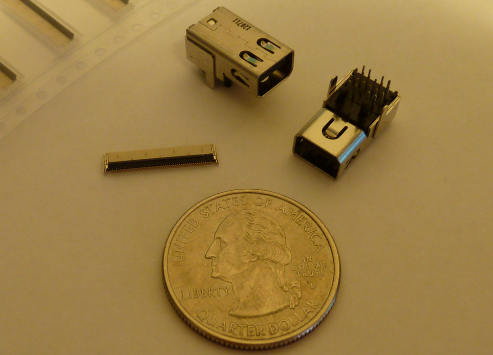
Teeny tiny.
As I mentioned in a previous post, I plan to manufacture these boards through OSH Park. They have somewhat stricter design rules than my usual board supplier, but they’re also less than 10% of the cost. The rules at time of this writing stipulate 6 mil trace, 6 mil space, with 13-mil min drill and 7-mil annular ring, and no plated slots.
Here’s the problem. The pins on a mDP connector are so tightly spaced that it’s hard to route with 6-mil traces, and because plated slots aren’t allowed, an even more roundabout path must be taken for Link 3 to avoid the now necessarily round shielding pads. I then spent a couple hours figuring out the optimal way to route the signals through the transient suppression diode array, got everything lined up and happily routed on one layer, and went to verify the orientation of the connector to the FFC, and…
Damn. The pin numbering of the FFC is opposite that of Molex’s numbering for the connector! Ugh! Now all of the signals are backward. And to maintain the desired relative orientation of the board to the FFC to the mDP, I cannot route it on a single layer anymore. I knew it was too good to be true.
So be it. The board is still routeable. Just now there are vias in the high-speed lines, which is generally a no-no. Well, you do what you gotta do. Here’s my plan of attack:
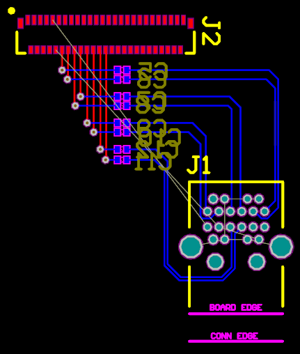
Veeery preliminary.
I always start a design this way, by planning out the routes with regular (non-diff-paired, non-length-matched) traces and rough part placement. Then I start a brand-new PCB and add in the parts and traces for real. That way I don’t waste so much time with tiny tweaks and shifts, which is easily the most time-consuming and least satisfying part of a design for me. So nobody write angry comments about mismatched trace lengths or pair separation, okay?
Every step of this process makes me more and more nervous about this design. The capacitors in the above layout are 0402 size. The occupied space is about one square inch. The board will of course be much larger than this once I add the backlight driver, but still… I always have a hard time visualizing just how small a design is until it’s actually in my hand. And this is easily the most intricate design I’ve yet done (most of what I do is big power stuff), so it should be even more surprising.
The work continues. Hopefully I will receive the panel within the next couple days and I can get some proper measurements.
<< Previous post in this series … Next post in this series >>
Hello, I am also looking to do something similar except I am going to make a LCD projector, is there any possibility of chipping in and getting another board? I just need the straight pass through cable as I am removing all of the panel except for the LCD.
Thanks in advance,
I have ordered a single set of boards (3) for this run, of which I will be using at least two (one to debug and test with, and one fully built-up). Whether it works or not, I will be ordering another set of boards somewhere along the line. I think we can probably work something out, if not for the third board from this set, at least for the next run. Would you need the components populated, or just a bare board?
You bring up an interesting topic – a lot of people seem to be intent on making these into projectors, which wouldn’t need the extra complexity that this board will have (controls, backlight driver, etc). Maybe it’s worthwhile to draw up a slimmed-down version of the board as well. I’ll ponder that.
I can populate the board myself if needed, I have solder re-flow gun and Hakko Iron. I would be interested in a stripped version.
I honestly think it would be fairly simple design as the only thing needed from the FFC molex is the DisplayPort signal. From what I have observed it may be more straight forward to just have a standard size Display Port connector, the boards would be quite tiny and easy to mass produce. I have no experience laying out PCBs or using CAD software… But from my electronics experience it should be nothing more than a straight pass through and maybe some very basic external LED power header that would be optional.
I’ll try to see about maybe laying something basic out.
You need to get power from somewhere. The DisplayPort specification actually notes that cable manufacturers should not route the DP_PWR signal, as it is only intended for converter dongles and such. If you get lucky or if the cable manufacturer is nice, you may be able to get power out of the cable, but it is not guaranteed.
I think you are right in that full-size DP is a good idea. There are not very many people making mDP headers – even Molex doesn’t admit to making the part that I ordered from them. I figured that mDP was the de-facto standard these days (definitely in the Apple world, and starting to continue into PCs), and I wanted to prevent the need for a converter dongle hanging off the back. Plus it cut down on the size of the board, which saves cost.
I might try my hand at a no-frills breakout if I get bored. My PCBs don’t get sent to the fabricator until the 15th so I have some time to kill.
I will have a PC power supply so pulling the 3.3v will not be an issue, I need the power supply for 12V for PC fans and water pump, I was under the impression that the benefit of the DP connector was that it was powered. Oh well. Everything I use has a full length DP connector so it would make things easier for me at least, but from what I looked at it also makes it easier to layout the board.
I had an hour to kill so I got a pretty good start on a simpler adapter. It’s not as easy as you may think – due to the numbering of DP vs the iPad LCD connector, the lines have to cross over so vias and a four-layer board are still necessary. The simplest way is to put the DP connector on one side of the board and the FFC on the other.
I’ll put out a formal post on it later.
I had that exact idea, anyways I look forward to your post!